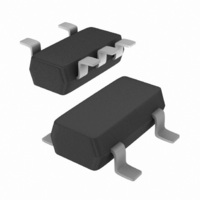
74AHC1G66GV,125 NXP Semiconductors, 74AHC1G66GV,125 Datasheet - Page 6

74AHC1G66GV,125
Manufacturer Part Number
74AHC1G66GV,125
Description
IC SWITCH SPST SC74A
Manufacturer
NXP Semiconductors
Series
74AHCr
Type
Analog Switchr
Datasheet
1.74AHC1G66GW165.pdf
(17 pages)
Specifications of 74AHC1G66GV,125
Package / Case
SC-74A, SOT-753
Function
Switch
Circuit
1 x SPST- NO
On-state Resistance
14 Ohm
Voltage Supply Source
Single Supply
Voltage - Supply, Single/dual (±)
2 V ~ 5.5 V
Current - Supply
1µA
Operating Temperature
-40°C ~ 125°C
Mounting Type
Surface Mount
Switch Configuration
SPST
On Resistance (max)
148 Ohm (Typ) @ 2 V
On Time (max)
35 ns @ 2 V
Off Time (max)
35 ns @ 2 V
Supply Voltage (max)
5.5 V
Supply Voltage (min)
2 V
Maximum Power Dissipation
250 mW
Maximum Operating Temperature
+ 125 C
Mounting Style
SMD/SMT
Minimum Operating Temperature
- 40 C
Package
5SOT-753
Maximum On Resistance
110@3.6V Ohm
Maximum Propagation Delay Bus To Bus
5@2V|2@3.6V|1@5.5V ns
Maximum Low Level Output Current
25 mA
Maximum Turn-on Time
35@2V ns
Switch Architecture
SPST
Power Supply Type
Single
Lead Free Status / RoHS Status
Lead free / RoHS Compliant
Lead Free Status / RoHS Status
Lead free / RoHS Compliant, Lead free / RoHS Compliant
Other names
74AHC1G66GV
74AHC1G66GV
935271669125
74AHC1G66GV
935271669125
NXP Semiconductors
Table 8.
At recommended operating conditions; voltages are referenced to GND (ground 0 V); for graph see
[1]
74AHC_AHCT1G66_4
Product data sheet
Symbol
74AHC1G66 and 74AHCT1G66
R
R
Fig 6.
ON(peak)
ON(rail)
At supply voltages approaching 2 V, the analog switch ON resistance becomes extremely non-linear. Therefore it is recommended that
these devices be used to transmit digital signals only, when using this supply voltage.
V
R
Test circuit for measuring ON resistance
Parameter
ON resistance
(peak)
ON resistance
(rail)
IH
ON
ON resistance
= V
V I
10.2 ON resistance
10.3 ON resistance test circuit and graphs
SW
/ I
E
Y
SW
.
Conditions
V
V
V
V
V
SW
CC
I
I
I
I
I
I
I
I
I
I
I
I
GND
= V
= GND; see
= V
SW
SW
SW
SW
SW
SW
SW
SW
SW
CC
CC
= 1.0 mA; V
= 10 mA; V
= 10 mA; V
= 1.0 mA; V
= 10 mA; V
= 10 mA; V
= 1.0 mA; V
= 10 mA; V
= 10 mA; V
Z
; see
to GND; see
Figure 6
001aag490
Figure 6
CC
CC
CC
CC
CC
CC
CC
CC
CC
Rev. 04 — 18 December 2008
= 3.0 V to 3.6 V
= 4.5 V to 5.5 V
= 3.0 V to 3.6 V
= 4.5 V to 5.5 V
= 3.0 V to 3.6 V
= 4.5 V to 5.5 V
I SW
= 2.0 V
= 2.0 V
= 2.0 V
Figure 6
74AHC1G66; 74AHCT1G66
Fig 7.
148
Typ
28
15
30
20
15
28
18
13
R
( )
25 C
ON
[1]
40
30
20
10
0
0
T
Typical ON resistance as a function of
input voltage
max
amb
50
30
50
22
50
22
-
-
-
= 25 C.
Single-pole single-throw analog switch
40 C to +85 C
Max
2
70
40
65
26
65
26
-
-
-
V
CC
= 3.0 V
Figure 7
40 C to +125 C Unit
4
4.5 V
© NXP B.V. 2008. All rights reserved.
V
Max
110
I
60
90
40
90
40
(V)
-
-
-
mna630
[1]
5.5 V
.
6
6 of 17


