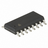
HI9P0508-9 Intersil, HI9P0508-9 Datasheet

HI9P0508-9
Specifications of HI9P0508-9
Related parts for HI9P0508-9
HI9P0508-9 Summary of contents
Page 1
... CAUTION: These devices are sensitive to electrostatic discharge; follow proper IC Handling Procedures. | 1-888-INTERSIL or 1-888-468-3774 Intersil (and design registered trademark of Intersil Americas Inc. Copyright © Intersil Americas Inc. 2003, 2005, 2007. All Rights Reserved All other trademarks mentioned are the property of their respective owners. FN3142.8 ...
Page 2
... HI3-0507-5Z HI3-507-5Z HI1-0508-2 HI1-508-2 HI1-0508-5 HI1-508 HI3-0508-5 HI3-508-5 HI3-0508-5Z (Note 1) HI3-508-5Z HI9P0508-5 HI9P508-5 HI9P0508-5Z (Notes 1, 2) HI9P508-5Z HI9P0508-9 HI9P508-9 HI9P0508-9Z (Note 1) HI9P508-9Z HI1-0509-2 HI1-509-2 HI1-0509-4 HI1-509-4 HI1-0509-5 HI1-509-5 HI3-0509-5 HI3-509-5 HI4P0509-5 HI4P 509-5 HI4P0509-5Z (Notes 1, 2) HI4P 509-5Z HI9P0509-5 HI9P 509-5 ...
Page 3
Pinouts HI-506 (CERDIP, SOIC) TOP VIEW +V 1 SUPPLY GND 12 NC ...
Page 4
Pinouts (Continued) HI-509 (PDIP, CERDIP, SOIC) TOP VIEW ENABLE SUPPLY OUT HI-506, HI-507, HI-508, HI-509 ...
Page 5
Truth Tables HI-506 ...
Page 6
Functional Diagrams HI-506 DECODER/ DRIVER LEVEL REF SHIFT † DIGITAL INPUT † † † † PROTECTION HI-508 DECODER/ DRIVER LEVEL ...
Page 7
Schematic Diagrams ENABLE OR A DELETE DELETE 200Ω TTL REFERENCE CIRCUIT P15 Q1P V L N12 D3 Q10N Q9P N13 N14 N15 V- ...
Page 8
... See Tech Brief TB379 for details Signals OUT exceeding are clamped by internal diodes. Limit resulting current to maximum current ratings overvoltage condition is anticipated (analog input exceeds either power supply voltage), the Intersil HI-546/HI-547/HI-548/HI-549 multiplexers are recommended. Electrical Specifications Supplies = +15V, -15V ...
Page 9
Electrical Specifications Supplies = +15V, -15V; V Unless Otherwise Specified. For Test Conditions, Consult Test Circuits Section (Continued) PARAMETER Input Leakage Current (High or Low ANALOG CHANNEL CHARACTERISTICS Analog Signal Range Resistance Δr ...
Page 10
Test Circuits and Waveforms 400 300 +125°C 200 +25°C 100 -55°C 0 -15 - ANALOG INPUT (V) FIGURE 1B. ON RESISTANCE vs ANALOG INPUT VOLTAGE 100nA OFF OUTPUT LEAKAGE CURRENT 10nA I D(OFF) 1nA OFF INPUT LEAKAGE CURRENT ...
Page 11
Test Circuits and Waveforms A I S(OFF) ±10V +10V FIGURE 2C. I TEST CIRCUIT (NOTE 12) S(OFF) NOTE: 12. Two measurements per channel: ±10V and +10V. (Two measurements per device for ...
Page 12
Test Circuits and Waveforms 600 400 200 LOGIC LEVEL (HIGH) (V) FIGURE 5A. ACCESS TIME vs LOGIC LEVEL (HIGH) 3.5V 50% +10V OUTPUT 10 FIGURE 5C. MEASUREMENT POINTS V † 12 HI-506, HI-507, ...
Page 13
Test Circuits and Waveforms 3.5V 0V 50% 50% t OPEN FIGURE 6B. MEASUREMENT POINTS V † 3.5V 50% 50% 90% t ON(EN) t OFF(EN) FIGURE 7B. MEASUREMENT POINTS 13 HI-506, HI-507, HI-508, HI-509 T = +25° ±15V, V ...
Page 14
Typical Performance Curves POWER SUPPLY VOLTAGE (±V) FIGURE 8. LOGIC THRESHOLD vs POWER SUPPLY VOLTAGE -55 -35 - TEMPERATURE (°C) ...
Page 15
Die Characteristics METALLIZATION: Type: CuAl Å Å Thickness: 16k ±2k SUBSTRATE POTENTIAL (NOTE): -V SUPPLY PASSIVATION: Type: Nitride/Silox Å Å Nitride Thickness: 3.5k ±1k Å Å Silox Thickness: 12k ±2k NOTE: The substrate appears resistive to the -V conductor at ...
Page 16
Die Characteristics METALLIZATION: Type: CuAl ±2k Å Å Thickness: 16k SUBSTRATE POTENTIAL (NOTE): -V SUPPLY PASSIVATION: Type: Nitride/Silox ±1k Å Å Nitride Thickness: 3.5k ±2k Å Å Silox Thickness: 12k NOTE: The substrate appears resistive to the -V conductor at ...
Page 17
Dual-In-Line Plastic Packages (PDIP INDEX N/2 AREA -B- -A- D BASE PLANE -C- SEATING PLANE 0.010 (0.25 NOTES: 1. Controlling Dimensions: INCH. In case of conflict between ...
Page 18
Dual-In-Line Plastic Packages (PDIP INDEX N/2 AREA -B- -A- D BASE PLANE -C- SEATING PLANE 0.010 (0.25 NOTES: 1. Controlling Dimensions: INCH. In case of conflict between ...
Page 19
Ceramic Dual-In-Line Frit Seal Packages (CERDIP) -D- -A- E -B- bbb BASE Q PLANE -C- SEATING PLANE aaa ccc ...
Page 20
Ceramic Dual-In-Line Frit Seal Packages (CERDIP) -D- -A- E -B- bbb BASE Q PLANE -C- SEATING PLANE aaa ccc ...
Page 21
Small Outline Plastic Packages (SOIC) N INDEX 0.25(0.010) H AREA E - SEATING PLANE - -C- α 0.10(0.004) 0.25(0.010 NOTES: 1. Symbols are defined in the ...
Page 22
Small Outline Plastic Packages (SOIC) N INDEX 0.25(0.010) H AREA E - SEATING PLANE - -C- α 0.10(0.004) 0.25(0.010 NOTES: 1. Symbols are defined in the ...
Page 23
Plastic Leaded Chip Carrier Packages (PLCC) 0.042 (1.07) 0.042 (1.07) 0.048 (1.22) 0.056 (1.42) PIN (1) IDENTIFIER 0.050 (1.27 0.020 (0.51) MAX 3 PLCS 0.026 (0.66) 0.032 (0.81) 0.045 (1.14) MIN VIEW “A” ...
Page 24
... Accordingly, the reader is cautioned to verify that data sheets are current before placing orders. Information furnished by Intersil is believed to be accurate and reliable. However, no responsibility is assumed by Intersil or its subsidiaries for its use; nor for any infringements of patents or other rights of third parties which may result from its use ...


