ISL59530IRZ Intersil, ISL59530IRZ Datasheet
ISL59530IRZ
Specifications of ISL59530IRZ
Available stocks


Related parts for ISL59530IRZ

ISL59530IRZ Summary of contents
Page 1
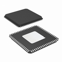
... IIntersil (and design trademark owned by Intersil Corporation or one of its subsidiaries. All other trademarks mentioned are the property of their respective owners. ISL59530 April 13, 2011 FN6220.8 PART PACKAGE MARKING (Pb-Free) ISL59530IKZ 356 Ld PBGA V356.27x27B ISL59530IRZ 72 Ld QFN L72.10x10C Copyright © Intersil Americas Inc. 2006-2008, 2011. All Rights Reserved. PKG. DWG. # ...
Page 2
Block Diagram V REF CLAMP 16 VIDEO INPUTS IN0 – IN15 CLAMP SDI SCLK SLATCH 2 ISL59530 V VOVERn S 16 OVERLAY VIDEO INPUTS 16x16 SWITCH MATRIX CLAMP X1, X2 ENABLE SPI INTERFACE AND CONTROL REGISTERS OVERn 16 OVERLAY CHANNEL ...
Page 3
Pinouts A In12 In13 In14 In11 SDO In10 SDO H Vs In9 RESET J Vs SLATCH K Vs In8 CLK L Vs SDI M Vs In7 V REF ...
Page 4
Pinouts (Continued GND 1 RESET IN11 5 IN10 IN9 8 IN8 9 SLATCH CLK 12 IN7 13 IN6 IN5 16 IN4 17 VS SDI ...
Page 5
... Maximum Die Temperature . . . . . . . . . . . . . . . . . . . . . . . . . . +125°C Storage Temperature . . . . . . . . . . . . . . . . . . . . . . . .-65°C to +150°C Pb-free reflow profile . . . . . . . . . . . . . . . . . . . . . . . . . see link below http://www.intersil.com/pbfree/Pb-FreeReflow.asp CAUTION: Do not operate at or near the maximum ratings listed for extended periods of time. Exposure to such conditions may adversely impact product reliability and result in failures not covered by warranty. ...
Page 6
AC Electrical Specifications V PARAMETER DESCRIPTION dG Diff Gain dP Diff Phase XT Adjacent Channel Crosstalk ADJACENT XT Hostile Crosstalk HOSTILE V Input Referred Noise Voltage N NOTE: 6. Compliance to datasheet limits is assured by one or more methods: ...
Page 7
Pin Descriptions (Continued QFN 356 LD PBGA 57 A15 59 B13 60 B11 - W10 - W12 - Y14 - Y16 - V19 - T19 - P20 - M20 - K19 - H19 - F20 - D20 - ...
Page 8
Pin Descriptions (Continued QFN 356 LD PBGA 10, 14, 17, 24, 25, D4, E4, F4, G4, H4, J4, 28, 32, 40, 43, ...
Page 9
Typical Performance Curves 15pF 100Ω L INPUT_CH 0 OUTPUT_CH 0 4.7pF FIGURE 1. FREQUENCY RESPONSE - VARIOUS C MUX MODE V =+ 1pF ...
Page 10
Typical Performance Curves 15pF 10pF 4.7pF 100Ω L INPUT_CH 0 OUTPUT_CH 0 FIGURE 7. FREQUENCY RESPONSE - VARIOUS C BROADCAST MODE ...
Page 11
Typical Performance Curves THD 2nd HD 3rd HD FIGURE 13. HARMONIC DISTORTION vs FREQUENCY FIGURE 15. DISABLED OUTPUT IMPEDANCE MUX MODE 100Ω L INPUT_CH 0 OUTPUT_CH 0 TIME (ns) FIGURE 17. RISE TIME - ...
Page 12
Typical Performance Curves MUX MODE 100Ω L INPUT_CH 0 OUTPUT_CH 0 TIME (ns) FIGURE 19. RISE TIME - A MUX MODE 100Ω L INPUT_CH 0 OUTPUT_CH 0 TIME ...
Page 13
Typical Performance Curves OUTPUT FIGURE 25. OVERLAY SWITCH TURN-ON DELAY TIME 100Ω L INPUT_CH 1 OUTPUT_CH 1 OSC = 40mV FIGURE 27. DIFFERENTIAL GAIN 100Ω L INPUT_CH ...
Page 14
Typical Performance Curves 100Ω L INPUT_CH 1 OUTPUT_CH1 OSC = 40mV FIGURE 31. DIFFERENTIAL GAIN 100Ω L INPUT_CH 1 OUTPUT_CH 1 OSC = 40mV FIGURE 33. DIFFERENTIAL ...
Page 15
Typical Performance Curves 100Ω L INPUT_CH 01 OUTPUT_CH 15 OSC = 40mV FIGURE 37. DIFFERENTIAL GAIN 100Ω L INPUT_CH 01 OUTPUT_CH 15 OSC = 40mV FIGURE 39. ...
Page 16
Typical Performance Curves 100Ω L INPUT_CH 01 OUTPUT_CH 01 OSC = 40mV FIGURE 43. DIFFERENTIAL GAIN, OVERLAY 100Ω L INPUT_CH 01 OUTPUT_CH 01 OSC = 40mV FIGURE ...
Page 17
Bandwidth, MUX Mode 255 229 229 1 244 217 2 257 235 3 264 4 255 5 253 6 247 7 253 227 235 8 255 236 240 9 241 10 235 11 ...
Page 18
Bandwidth, Broadcast Mode 215 198 195 1 214 195 2 210 188 3 212 4 206 5 203 6 201 7 204 187 182 8 204 187 183 9 202 10 196 11 194 ...
Page 19
Block Diagram V REF CLAMP 16 VIDEO INPUTS IN0 – IN15 CLAMP SDI SCLK SLATCH General Description The ISL59530 is a 16x16 integrated video crosspoint switch matrix with input and output buffers and On-Screen Display (OSD) insertion. This device operates ...
Page 20
Serial Timing Diagram SLATCH SCLK SDI (LSB) B0 SDO (PREVIOUS) )(PREVIOUS) SDO = SDI delayed by 15.5 SCLKs to allow daisy-chaining of multiple ISL59530s. SDO changes on the falling edge of SCLK. PARAMETER RECOMMENDED OPERATING ...
Page 21
Enabling Outputs The output enable control word is used to enable individual outputs. There are 16 channels to configure, so this is accomplished by writing 4 serial words, each controlling a bank of four outputs at a time. The bank ...
Page 22
For this reason, the ISL59530 must be in DC-coupled mode (Clamp Disabled compatible with S-video and component video signals. Bandwidth Considerations Wide frequency response (high bandwidth video system means better video resolution. Four sets of frequency ...
Page 23
~0.4V REF Q 1 (110µ SS12 0.1µF INx VIDEO IN C 0.1µ FIGURE 49. DC-RESTORE BLOCK DIAGRAM This is how the video is “DC-restored” after being AC-coupled ...
Page 24
... Accordingly, the reader is cautioned to verify that data sheets are current before placing orders. Information furnished by Intersil is believed to be accurate and reliable. However, no responsibility is assumed by Intersil or its subsidiaries for its use; nor for any infringements of patents or other rights of third parties which may result from its use ...
Page 25
Package Outline Drawing L72.10x10C 72 LEAD QUAD FLAT NO-LEAD PLASTIC PACKAGE (PUNCH QFN) Rev 0, 7/07 10.00 9. PIN 1 INDEX AREA (4X) 0.15 TOP VIEW PACKAGE OUTLINE 6.00 10.00 TYPICAL RECOMMENDED LAND PATTERN 11° ±1° ALL ...
Page 26
Package Outline Drawing V356.27x27B 356 BALL PLASTIC BALL GRID ARRAY PACKAGE (PBGA) Rev 2, 10/10 27.00 24.00 +0.35 -0.05 A1 BALL 4X 10.00 PAD CORNER 5. A1 BALL PAD INDICATOR, 1.0 DIA., OPTIONAL 4X 45° TOP VIEW CHAMFER 1.27 TYPICAL ...