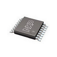
PCA9546PW NXP Semiconductors, PCA9546PW Datasheet - Page 10

PCA9546PW
Manufacturer Part Number
PCA9546PW
Description
Manufacturer
NXP Semiconductors
Datasheet
1.PCA9546PW.pdf
(17 pages)
Specifications of PCA9546PW
Logical Function
I2C Multiplexer
Configuration
1 x 4:1
Number Of Inputs
4
Number Of Outputs
1
Operating Supply Voltage (typ)
2.5/3.3/5V
Operating Supply Voltage (min)
2.3V
Operating Supply Voltage (max)
5.5V
Power Dissipation
400mW
Operating Temp Range
-40C to 85C
Operating Temperature Classification
Industrial
Mounting
Surface Mount
Pin Count
16
Package Type
TSSOP
Lead Free Status / Rohs Status
Compliant
Available stocks
Company
Part Number
Manufacturer
Quantity
Price
Part Number:
PCA9546PW
Manufacturer:
PHILIPS/飞利浦
Quantity:
20 000
1. Stresses beyond those listed may cause permanent damage to the device. These are stress ratings only and functional operation of the
2. The performance capability of a high-performance integrated circuit in conjunction with its thermal environment can create junction
Philips Semiconductors
ABSOLUTE MAXIMUM RATINGS
In accordance with the Absolute Maximum Rating System (IEC 134).Voltages are referenced to GND (ground = 0 V).
NOTES:
DC CHARACTERISTICS
V
2004 Sep 30
Supply
Input SCL; input/output SDA
Select inputs A0 to A2 / RESET
Pass Gate
DD
SYMBOL
SYMBOL
4-channel I
device at these or any other conditions beyond those indicated under “recommended operating conditions” is not implied. Exposure to
absolute-maximum-rated conditions for extended periods may affect device reliability.
temperatures which are detrimental to reliability. The maximum junction temperature of this integrated circuit should not exceed 150 C.
SYMBOL
V
V
V
R
R
V
= 2.3 V to 3.6 V; V
I
V
V
I
V
I
I
V
C
Pass
POR
I
DD
stb
O
OL
C
C
T
I
I
DD
O
ON
V
LI
T
IH
L
IH
L
I
P
IL
IL
I
io
amb
V
I
DD
SS
i
i
DD
I
stg
O
tot
I
I
Supply voltage
Supply current
Standby current
Power-on reset voltage
LOW-level input voltage
HIGH-level input voltage
LOW level output current
LOW-level output current
Leakage current
Input capacitance
LOW-level input voltage
HIGH-level input voltage
Input leakage current
Input capacitance
Switch resistance
Switch resistance
Switch output voltage
Switch output voltage
Leakage current
Input/output capacitance
DC supply voltage
DC input voltage
DC input current
DC output current
Supply current
Supply current
total power dissipation
Storage temperature range
Operating ambient temperature
PARAMETER
PARAMETER
2
SS
C switch with reset
= 0 V; T
PARAMETER
amb
= –40 C to +85 C; unless otherwise specified. (See page 11 for V
1, 2
V
V
V
swin
swin
CC
V
V
V
CC
= 2.3 V to 2.7 V; V
swin
swin
= V
= V
Operating mode; V
Standby mode; V
= 3.67 V; V
DD
DD
no load; V
= V
= V
no load; V
no load; V
TEST CONDITIONS
TEST CONDITIONS
= 3.0 V to 3.6 V; I
= 2.3 V to 2.7 V; I
DD
DD
pin at V
V
V
f
SCL
I
I
= 3.3 V; I
= 2.5 V; I
V
V
= V
= V
OL
OL
V
V
V
I
I
I
O
I
= 100 kHz
I
I
DD
DD
= V
= V
= V
= V
= 0.4 V
= 0.6 V
DD
= V
= V
= 0.4 V; I
10
O
or V
or V
DD
SS
SS
SS
or V
CONDITIONS
DD
DD
swout
swout
DD
= 0.4V; I
DD
or V
SS
SS
or V
or V
= 3.6 V;
SS
= 3.6 V;
swout
swout
O
= –100 A
= –100 A
SS
SS
SS
= 15 mA
O
;
= –100 A
= –100 A
= 10 mA
0.7V
0.7V
MIN
–0.5
–0.5
2.3
1.6
1.1
–1
–1
–1
—
—
—
—
—
—
—
—
3
6
5
7
DD
DD
DD
= 3.6 V to 5.5 V)
–0.5 to +7.0
–0.5 to +7.0
–60 to +150
LIMITS
–40 to +85
TYP
RATING
1.6
1.6
2.2
1.5
40
20
12
20
26
—
—
—
—
—
—
—
—
—
—
—
—
3
400
100
100
20
25
V
+0.3V
0.3V
DD
MAX
PCA9546
100
100
3.6
2.1
2.8
2.0
Product data sheet
+1
13
+1
30
55
+1
—
—
—
—
6
3
5
+ 0.5
DD
DD
UNIT
mW
mA
mA
mA
mA
UNIT
UNIT
V
V
C
C
mA
mA
pF
pF
pF
V
V
V
V
V
V
V
V
A
A
A
A
A


