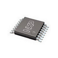
PCA9546PW NXP Semiconductors, PCA9546PW Datasheet - Page 8

PCA9546PW
Manufacturer Part Number
PCA9546PW
Description
Manufacturer
NXP Semiconductors
Datasheet
1.PCA9546PW.pdf
(17 pages)
Specifications of PCA9546PW
Logical Function
I2C Multiplexer
Configuration
1 x 4:1
Number Of Inputs
4
Number Of Outputs
1
Operating Supply Voltage (typ)
2.5/3.3/5V
Operating Supply Voltage (min)
2.3V
Operating Supply Voltage (max)
5.5V
Power Dissipation
400mW
Operating Temp Range
-40C to 85C
Operating Temperature Classification
Industrial
Mounting
Surface Mount
Pin Count
16
Package Type
TSSOP
Lead Free Status / Rohs Status
Compliant
Available stocks
Company
Part Number
Manufacturer
Quantity
Price
Part Number:
PCA9546PW
Manufacturer:
PHILIPS/飞利浦
Quantity:
20 000
Philips Semiconductors
Acknowledge
The number of data bytes transferred between the start and the stop conditions from transmitter to receiver is not limited. Each byte of eight bits
is followed by one acknowledge bit. The acknowledge bit is a HIGH level put on the bus by the transmitter whereas the master generates an
extra acknowledge related clock pulse.
A slave receiver which is addressed must generate an acknowledge after the reception of each byte. Also a master must generate an
acknowledge after the reception of each byte that has been clocked out of the slave transmitter. The device that acknowledges has to pull down
the SDA line during the acknowledge clock pulse, so that the SDA line is stable LOW during the HIGH period of the acknowledge related clock
pulse, set-up and hold times must be taken into account.
A master receiver must signal an end of data to the transmitter by not generating an acknowledge on the last byte that has been clocked out of
the slave. In this event, the transmitter must leave the data line HIGH to enable the master to generate a stop condition.
2004 Sep 30
4-channel I
BY TRANSMITTER
DATA OUTPUT
2
DATA OUTPUT
BY RECEIVER
C switch with reset
SCL FROM
SDA
SDA
MASTER
start condition
start condition
S
S
START condition
1
1
S
1
1
SLAVE ADDRESS
1
SLAVE ADDRESS
1
Figure 9. Acknowledgement on the I
0
0
A2
A2
Figure 10. WRITE control register
Figure 11. READ control register
1
A1
A1
A0
A0
R/W
1
R/W
0
2
A
acknowledge
from slave
A
acknowledge
from slave
8
X
X
X
CONTROL REGISTER
not acknowledge
CONTROL REGISTER
X
X
acknowledge
X
X
8
X
2
B3
C-bus
B3
B2
B2
no acknowledge
from master
B1
acknowledge
from slave
B1
9
B0
B0
last byte
NA
SW00917
A
P
stop condition
P
clock pulse for
acknowledgement
SW00918
PCA9546
Product data sheet
SW00368


