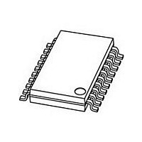
TDA8547TS NXP Semiconductors, TDA8547TS Datasheet - Page 8

TDA8547TS
Manufacturer Part Number
TDA8547TS
Description
The TDA8547TS is a two channel audio power amplifierfor an output power of 2 x 0
Manufacturer
NXP Semiconductors
Datasheet
1.TDA8547TS.pdf
(21 pages)
Specifications of TDA8547TS
Operational Class
Class-AB
Audio Amplifier Output Configuration
2-Channel Stereo
Output Power (typ)
1.2x2@8OhmW
Audio Amplifier Function
Speaker
Total Harmonic Distortion
0.15@8Ohm@0.4W%
Single Supply Voltage (typ)
5V
Dual Supply Voltage (typ)
Not RequiredV
Power Supply Requirement
Single
Power Dissipation
1.1W
Rail/rail I/o Type
No
Single Supply Voltage (min)
2.2V
Single Supply Voltage (max)
18V
Dual Supply Voltage (min)
Not RequiredV
Dual Supply Voltage (max)
Not RequiredV
Operating Temp Range
-40C to 85C
Operating Temperature Classification
Industrial
Mounting
Surface Mount
Pin Count
20
Package Type
SSOP
Dc
10+
Lead Free Status / Rohs Status
Compliant
Available stocks
Company
Part Number
Manufacturer
Quantity
Price
Company:
Part Number:
TDA8547TS/N1
Manufacturer:
NXP
Quantity:
1 000
Company:
Part Number:
TDA8547TS/N1Ј¬118
Manufacturer:
NXP
Quantity:
10 000
NXP Semiconductors
AC CHARACTERISTICS
V
unless otherwise specified.
Notes
1. Gain of the amplifier is
2. The noise output voltage is measured at the output in a frequency range from 20 Hz to 20 kHz (unweighted), with a
3. Supply voltage ripple rejection is measured at the output, with a source impedance of R
4. Supply voltage ripple rejection is measured at the output, with a source impedance of R
5. Output voltage in mute position is measured with a 1 V (RMS) input voltage in a bandwidth of 20 Hz to 20 kHz,
6. Channel separation is measured at the output with a source impedance of R
1998 Apr 01
P
THD
G
Z
V
SVRR
V
α
CC
i
cs
o
no
o
2 × 0.7 W BTL audio amplifier with
output channel switching
v
SYMBOL
source impedance of R
The ripple voltage is a sine wave with a frequency of 1 kHz and an amplitude of 100 mV (RMS), which is applied to
the positive supply rail.
The ripple voltage is a sine wave with a frequency between 100 Hz and 20 kHz and an amplitude of 100 mV (RMS),
which is applied to the positive supply rail.
so including noise.
1 kHz. The output power in the operating channel is set to 0.5 W.
= 5 V; T
amb
output power, one channel
total harmonic distortion
closed loop voltage gain
differential input impedance
noise output voltage
supply voltage ripple rejection
output voltage
channel separation
= 25 °C; R
L
S
2
= 8 Ω; f = 1 kHz; V
PARAMETER
= 0 Ω at the input.
×
R2
------- -
R1
in BTL application circuit Fig.4.
MODE
= 0 V; gain = 20 dB; measured in BTL application circuit Fig.4;
THD = 10%
THD = 0.5%
P
note 1
note 2
note 3
note 4
note 5
V
o
SELECT
8
= 0.4 W
CONDITIONS
= 0.5V
CC
; note 6 40
S
= 0 Ω at the input and a frequency of
1
0.6
−
6
−
−
50
40
−
MIN.
S
S
1.2
0.9
0.15
−
100
−
−
−
−
−
= 0 Ω at the input.
= 0 Ω at the input.
TYP.
TDA8547TS
Product specification
−
−
0.3
30
−
100
−
−
200
−
MAX.
W
W
%
dB
kΩ
μV
dB
dB
μV
dB
UNIT


