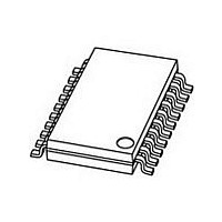
TDA8547TS NXP Semiconductors, TDA8547TS Datasheet - Page 9

TDA8547TS
Manufacturer Part Number
TDA8547TS
Description
The TDA8547TS is a two channel audio power amplifierfor an output power of 2 x 0
Manufacturer
NXP Semiconductors
Datasheet
1.TDA8547TS.pdf
(21 pages)
Specifications of TDA8547TS
Operational Class
Class-AB
Audio Amplifier Output Configuration
2-Channel Stereo
Output Power (typ)
1.2x2@8OhmW
Audio Amplifier Function
Speaker
Total Harmonic Distortion
0.15@8Ohm@0.4W%
Single Supply Voltage (typ)
5V
Dual Supply Voltage (typ)
Not RequiredV
Power Supply Requirement
Single
Power Dissipation
1.1W
Rail/rail I/o Type
No
Single Supply Voltage (min)
2.2V
Single Supply Voltage (max)
18V
Dual Supply Voltage (min)
Not RequiredV
Dual Supply Voltage (max)
Not RequiredV
Operating Temp Range
-40C to 85C
Operating Temperature Classification
Industrial
Mounting
Surface Mount
Pin Count
20
Package Type
SSOP
Dc
10+
Lead Free Status / Rohs Status
Compliant
Available stocks
Company
Part Number
Manufacturer
Quantity
Price
Company:
Part Number:
TDA8547TS/N1
Manufacturer:
NXP
Quantity:
1 000
Company:
Part Number:
TDA8547TS/N1Ј¬118
Manufacturer:
NXP
Quantity:
10 000
NXP Semiconductors
TEST AND APPLICATION INFORMATION
Test conditions
Because the application can be either Bridge-Tied Load
(BTL) or Single-Ended (SE), the curves of each
application are shown separately.
The thermal resistance = 110 K/W for the SSOP20; the
maximum sine wave power dissipation for T
is:
For T
Thermal Design Considerations
The ‘measured’ thermal resistance of the IC package is
highly dependent on the configuration and size of the
application board. Data may not be comparable between
different Semiconductor manufacturers because the
application boards and test methods are not (yet)
standardized. Also, the thermal performance of packages
for a specific application may be different than presented
here, because the configuration of the application boards
(copper area!) may be different. NXP Semiconductors
uses FR-4 type application boards with 1 oz copper
traces with solder coating.
The SSOP package has improved thermal conductivity
which reduces the thermal resistance. Using a practical
PCB layout (see Fig.24) with wider copper tracks to the
corner pins and just under the IC, the thermal resistance
from junction to ambient can be reduced to about 80 K/W.
For T
this PCB layout is:
Please note that this two channel IC is mentioned for
application with only one channel active. For that reason
the curves for worst case power dissipation are given for
the condition of only one of the both channels driven with
a 1 kHz sine wave signal.
BTL application
T
f = 1 kHz, R
22 Hz to 22 kHz.
The BTL application circuit is illustrated in Fig.4.
1998 Apr 01
150 60
--------------------- -
amb
2 × 0.7 W BTL audio amplifier with
output channel switching
110
150 25
--------------------- -
–
amb
= 25 °C if not specially mentioned, V
amb
110
–
= 60 °C the maximum total power dissipation is:
= 60 °C the maximum total power dissipation at
=
L
0.82 W
=
= 8 Ω, G
1.14 W
150 60
--------------------- -
80
v
–
= 20 dB, audio band-pass
=
1.12 W
CC
amb
= 5 V,
= 25 °C
9
The quiescent current has been measured without any
load impedance and both channels driven. When one
channel is active the quiescent current will be halved.
The total harmonic distortion as a function of frequency
was measured using a low-pass filter of 80 kHz.
The value of capacitor C3 influences the behaviour of the
SVRR at low frequencies: increasing the value of C3
increases the performance of the SVRR.
The figure of the MODE voltage (V
the supply voltage shows three areas; operating, mute
and standby. It shows, that the DC-switching levels of the
mute and standby respectively depend on the supply
voltage level. The figure of the SELECT voltage (V
as a function of the supply voltage shows the voltage
levels for switching the channels in the active, mute or
standby mode.
SE application
T
f = 1 kHz, R
22 Hz to 22 kHz.
The SE application circuit is illustrated in Fig.16.
Increasing the value of electrolytic capacitor C3 will result
in a better channel separation. Because the positive
output is not designed for high output current (2 × I
low load impedance (≤16 Ω), the SE application with
output capacitors connected to ground is advised.
The capacitor value of C6/C7 in combination with the load
impedance determines the low frequency behaviour.
The THD as a function of frequency was measured using
a low-pass filter of 80 kHz. The value of capacitor C3
influences the behaviour of the SVRR at low frequencies:
increasing the value of C3 increases the performance of
the SVRR.
General remark
The frequency characteristic can be adapted by
connecting a small capacitor across the feedback
resistor. To improve the immunity to HF radiation in radio
circuit applications, a small capacitor can be connected in
parallel with the feedback resistor (56 kΩ); this creates a
low-pass filter.
amb
= 25 °C if not specially mentioned, V
L
= 4 Ω, G
v
= 20 dB, audio band-pass
MODE
TDA8547TS
Product specification
) as a function of
CC
= 7.5 V,
SELECT
o
) at
)


