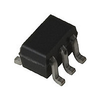
MGA83563TR1 Avago Technologies US Inc., MGA83563TR1 Datasheet

MGA83563TR1
Specifications of MGA83563TR1
Related parts for MGA83563TR1
MGA83563TR1 Summary of contents
Page 1
MGA-83563 +22 dBm P 3V Power Amplifier SAT for 0.5 – 6 GHz Applications Data Sheet Description Avago’s MGA-83563 is an easy-to-use GaAs RFIC amplifier that offers excellent power output and efficiency. This part is targeted for 3V applications where ...
Page 2
MGA-83563 Absolute Maximum Ratings Symbol Parameter V Maximum DC Supply Voltage Input Power in T Channel Temperature ch T Storage Temperature STG 3. 2 1.2 nH INPUT Figure 1. ...
Page 3
MGA-83563 Electrical Specifications, Symbol Parameters and Test Conditions P Saturated Output Power SAT PAE Power Added Efficiency [3,5] I Device Current d Gain Small Signal Gain P Saturated Output Power SAT PAE Power Added Efficiency P Output Power at 1 ...
Page 4
MGA-83563 Typical Performance 3.3V 12 3.0V 2. FREQUENCY (GHz) Figure 3. Tuned Gain vs. Frequency and Voltage -40C ...
Page 5
MGA-83563 Typical Performance, continued 2.7V 3.0V 22 3. INPUT POWER (dBm) @ 2.4 GHz Figure 12. Output Power vs. Input Power and ...
Page 6
MGA-83563 Test Circuit Typical s-parameters are shown below for various inductor values (L). Those marked “Sim” are simulated and those marked “Meas” are measured using an ICM (Inter- continental Microwave) fixture. Figure 17 shows the available gain for each L ...
Page 7
MGA-83563 Applications Information The MGA-83563 is two-stage, medium power GaAs RFIC amplifier designed to be used for driver and output stages in transmitter applications operating within the 500 MHz to 6 GHz frequency range. This device is designed for operation ...
Page 8
FREQUENCY (GHz) Figure 19. Values for Interstage Inductor L2. In order to prevent loss of output power, the value of the ...
Page 9
Choose a circuit topology that will match * as well as the range of im- ml pedances on the low side Beginning with this ml small signal output match, tune the circuit ...
Page 10
Adequate RF grounding is critical to obtain maximum per formance and to maintain device stability. All of the ground pins of the RFIC should be connected to the RF groundplane on the backside of the PCB by means of plated ...
Page 11
The channel-to-case thermal resistance (T the table of Absolute Maximum Ratings is 175°C/watt. Note that the meaning of “case” for packages such as the SOT-363 is defined as the interface between the package pins and the mounting surface, i.e., at ...
Page 12
Output Match The design of the small signal output matching circuit begins with the calculation of the small signal match im- pedance The set of S-parameters in Table 1 for an ml inductor value of 1 ...
Page 13
Input Match The input return loss without any external matching was measured as 7.6 dB (2.4:1 VWSR). For many applications no further matching is necessary. If, however, an im- proved input match is required, a simple series inductor is all ...
Page 14
OUTPUT -5 -10 -15 INPUT -20 -25 2 2.2 2.4 2.6 2.8 3 FREQUENCY (GHz) Figure 30. Input and Output Return Loss of the Completed 2.5 GHz Amplifier. Table 2 summarizes measured results for this particular amplifier at 2.5 GHz. ...
Page 15
Amplifier Designs for 1.9 GHz and 900 MHz The same design process used for the 2.5 GHz amplifier above was repeated for the design of amplifiers for the 1.9 GHz and 900 MHz frequency bands. Example circuits were built using ...
Page 16
MHz Amplifier Measured Results Measured results for this 900 MHz amplifier is shown in Table 4. The PAE is 40%. Output Mode Gain Power (dB) (dBm) Small Signal 24.5 — G 23.5 20.9 -1dB Saturated 18.5 22.5 Table 4. ...
Page 17
Summary of Example Amplifiers A schematic diagram for the three example amplifiers covering 2.5 GHz, 1.9 GHz, and 900 MHz is shown in Figure 38. Component values for the three designs are summarized in Table 5. Frequency (nH, pF) 900 ...
Page 18
Hints and Troubleshooting Oscillation Unconditional stability of the MGA-83563 is dependent on having good grounding. Inadequate device ground- ing or poor PCB layout techniques could cause the device to be potentially unstable multistage RFIC such as the MGA-83563, ...
Page 19
Appendix —Determination of Interstage Inductor Value. A methodology is presented here for determining the value of the interstage inductor, L2 that produces optimum large signal performance at any frequency. This is the method used to create the plot of Optimum ...
Page 20
Plot B provides a look-up for values of L2 for saturated amplifier designs. Plot A is used for linear amplifiers. Note: Plot B is replicated as Figure 19 in the “Application Guidelines” section of this note. [1] Operating life test ...
Page 21
Package Dimensions Outline 63 (SOT-363/SC-70 DIMENSIONS (mm) SYMBOL MIN. MAX. E 1.15 1.35 D 1.80 2.25 HE 1.80 2.40 A 0.80 1.10 A2 0.80 1.00 A1 0.00 0.10 Q1 0.10 0.40 e 0.650 BCS ...
Page 22
Device Orientation REEL USER FEED DIRECTION COVER TAPE Tape Dimensions and Product Orientation For Outline (CARRIER TAPE THICKNESS) 1 10° MAX DESCRIPTION SYMBOL CAVITY LENGTH A WIDTH B DEPTH K PITCH P ...


