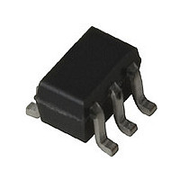
MGA83563TR1 Avago Technologies US Inc., MGA83563TR1 Datasheet - Page 9

MGA83563TR1
Manufacturer Part Number
MGA83563TR1
Description
Manufacturer
Avago Technologies US Inc.
Datasheet
1.MGA83563TR1.pdf
(22 pages)
Specifications of MGA83563TR1
Manufacturer's Type
Power Amplifier
Number Of Channels
1
Supply Current
200@3VmA
Frequency (max)
6GHz
Operating Supply Voltage (typ)
3V
Package Type
SOT-363
Mounting
Surface Mount
Pin Count
6
Lead Free Status / Rohs Status
Not Compliant
9
impedance will generally become lower. Choose a circuit
topology that will match *
pedances on the low side of *
small signal output match, tune the circuit under large
signal conditions for maximum saturated output power
and best efficiency.
It should be noted that both the saturated output power
(P
83563 is 100% RF tested at 2.4 GHz in a production test
fixture that simulates an actual amplifier application.
This method of testing not only guarantees minimum
performance standards, but also ensures repeatable RF
performance in the user’s production circuits.
Step 4 (Optional) — Input Impedance Match
As previously noted, the internal input impedance match
to the MGA-83563 is already reasonably good (return
loss is typically 8 dB) and may be adequate for many ap-
plications as is. The design of the MGA-83563 is such that
the second stage will enter into compression before the
first stage. The isolation provided by the first stage there-
fore results in a minimal impact on the input matching as
the amplifier becomes saturated.
If an improved input return loss is needed, an input circuit
is designed to match 50 Ω to *
cient of the source impedance for a conjugate match at
the input of the MGA-83563). The value of *
lated from the S-parameters in Table 1 in the same way
as was done for *
pedance to the MMIC is near 50 Ω and the reactive part
is capacitive, the addition of a simple series inductor is
often all that is needed if a better input match is required.
PCB Layout Recommendations
When laying out a printed circuit board for the MGA-
83563, several points should be taken into account. The
PCB layout will be a balance of electrical, thermal, and
assembly considerations.
Package Footprint
A recommended printed circuit board footprint for the
miniature SOT-363 (SC-70) package that is used by the
MGA-83563 is shown in Figure 20.
This package footprint provides ample allowance for
package placement by automated assembly equipment
without adding parasitics that could impair the high fre-
quency performance of the MGA-83563. (The padprint
in Figure 20 is shown with the footprint of a SOT-363
package superimposed on the PCB pads for reference.)
sat
) and power-added efficiency (PAE) for each MGA-
ml
. Since the real part of the input im-
ml
as well as the range of im-
ms
ml
. Beginning with this
(the reflection coeffi-
ms
is calcu-
PCB Materials
FR-4 or G-10 printed circuit board type of material is a
good choice for most low cost wireless applications for
frequencies through 3 GHz. Typical single-layer board
thickness is 0.020 to 0.031 inches. Multi-layer boards
generally use a dielectric layer thickness in the 0.005 to
0.010 inch range.
For higher frequency applications, e.g., 5.8 GHz, circuit
boards made with PTFE/glass dielectric materials are
suggested.
0.035
Figure 20. Recommended PCB Pad Layout for
Avago’s SC70 6L/SOT-363 Products.
RF Considerations
Starting with the package padprint of Figure 20, the
nucleus of a PCB layout is shown in Figure 21. This layout
is a good general purpose starting point for designs
using the MGA-83563 amplifier.
Input
Figure 21. Basic PCB Layout.
This layout is a microstripline design (solid groundplane
on the backside of the circuit board) with a 50 Ω input and
output and provision for inductor L2 with its bypass capaci-
tor.
RF
0.026
V
83
0.016
d1
0.075
Capacitor
L2
Bypass
Output
RF


