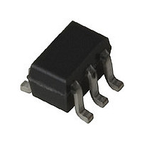
MGA83563TR1 Avago Technologies US Inc., MGA83563TR1 Datasheet - Page 12

MGA83563TR1
Manufacturer Part Number
MGA83563TR1
Description
Manufacturer
Avago Technologies US Inc.
Datasheet
1.MGA83563TR1.pdf
(22 pages)
Specifications of MGA83563TR1
Manufacturer's Type
Power Amplifier
Number Of Channels
1
Supply Current
200@3VmA
Frequency (max)
6GHz
Operating Supply Voltage (typ)
3V
Package Type
SOT-363
Mounting
Surface Mount
Pin Count
6
Lead Free Status / Rohs Status
Not Compliant
12
Output Match
The design of the small signal output matching circuit
begins with the calculation of the small signal match im-
pedance, *
inductor value of 1.2 nH is used since this is the closest
value to the 1.5 nH that was chosen for L2 in the first
design step.
Avago’s Touchstone program was used to interpolate the
s-parameter data and calculate a *
2.5 GHz.
This *
as Point C, along with an indication of the area of lower
impedance from this point. (The output impedance is
expected to decrease under large signal conditions.) A
two-element matching network consisting of a shunt ca-
pacitor and series transmission line is chosen to match
the output to 50 ohms.
-0.2
Figure 23. Initial Output Match for Small Signal.
The shunt-C, series-line topology is chosen based on its
ability to cover the expected range of impedance to be
matched and because it will pass DC bias into the output
pin of the MGA-83563. (For the latter reason, impedance
matching circuits using series capacitors are avoided.)
In some cases, it may be more practical to implement
the series transmission line element with a chip inductor.
If the series line is excessively long, the cost of an addi-
tional chip component can be traded off against circuit
board space. The substitution of an open-circuit line for
the shunt C may also be possible, thus eliminating the a
capacitor.
0.2
LARGE SIGNAL
ml
-0.5
0.5
point is plotted on the Smith chart in Figure 23
Output
RF
C (Γ
ml
. The set of S-parameters in Table 1 for an
ml
C
)
MLIN
B
1
-1
1
A
B
C
A (50 Ω)
2
2
-2
ml
of 0.14 ‘172° for
Input
Referring to the Smith chart in Figure 23, the initial output
match for *
tor followed by a 0.32-inch length of 50 : microstripline.
DC Bias
A 22 nH RFC is added to the 50 : side of the output
matching circuit to apply bias voltage to the drain of the
second stage. The RFC is bypassed with a 62 pF capacitor.
A series DC blocking capacitor, also 62 pF, is added to the
RF output to complete the bias circuit.
Optimizing the Output Match
To reach the final output matching circuit for maximum
saturated output power, an input power of +4 dBm
is applied to saturate the amplifier circuit. The output
matching circuit is then experimentally optimized by ad-
justing the value of the shunt capacitor and the distance
the capacitor is located along the output line from the
MGA-83563.
During the tuning process, the saturated output power
of the amplifier is monitored with a power meter con-
nected to the amplifier’s output. An ammeter is used to
observe total device DC current drain (I
tion of amplifier efficiency. The desired output match is
then achieved at the tuning point of maximum P
minimum I
The optimum output match for 2.5 GHz was achieved
with a shunt capacitor value of 0.9 pF located 0.08 inches
along the 50 Ω line from the output pin of the MGA-
83563. The final output circuit is shown in Figure 24.
Figure 24. Final RF Output Match for the 2.5 GHz Amplifier Tuned for
Maximum P
When tuned for maximum saturated output power, the
small signal output return loss for the amplifier was mea-
sured as 5.5 dB at 2.5 GHz.
RF
MGA-
83563
sat
.
d
ml
.
was determined to be a 0.4 pF shunt capaci-
0.08 in.
50 Ω
0.9 pF
Output
RF
d
) as an indica-
sat
and


