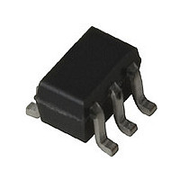
MGA83563TR1 Avago Technologies US Inc., MGA83563TR1 Datasheet - Page 10

MGA83563TR1
Manufacturer Part Number
MGA83563TR1
Description
Manufacturer
Avago Technologies US Inc.
Datasheet
1.MGA83563TR1.pdf
(22 pages)
Specifications of MGA83563TR1
Manufacturer's Type
Power Amplifier
Number Of Channels
1
Supply Current
200@3VmA
Frequency (max)
6GHz
Operating Supply Voltage (typ)
3V
Package Type
SOT-363
Mounting
Surface Mount
Pin Count
6
Lead Free Status / Rohs Status
Not Compliant
10
Adequate RF grounding is critical to obtain maximum
per formance and to maintain device stability. All of the
ground pins of the RFIC should be connected to the RF
groundplane on the backside of the PCB by means of
plated through holes (vias) that are placed very near
the package terminals. As a minimum, one via should
be located next to each ground pin to ensure good RF
grounding. It is a good practice to use multiple vias as in
Figure 21 to further minimize ground path inductance.
While it might be considered an effective RF practice, it
is recommended that the PCB pads for the ground pins
not be connected together underneath the body of the
package for two reasons. The first reason is that connect-
ing the ground pins of multi-stage amplifiers together
can sometimes result in undesirable feedback between
stages. Each ground pin should have its own indepen-
dent path to ground. The second reason is that PCB
traces hidden under the package cannot be adequately
inspected for solder quality.
Thermal Considerations
The DC power dissipation of the MGA-83563, which can
be on the order of 0.5 watt, is approaching the thermal
limits of subminiature packaging such as the SOT-363. As
a result, particular care should be taken to adequately
heatsink the MGA-83563.
The primary heat path from the MMIC chip to the
system heatsink is by means of conduction through the
package leads and ground vias to the groundplane on
the backside of the PCB. As previously mentioned in the
“PCB Layout” section, the use of multiple vias near all of
the ground pins is desirable for low inductance. The use
of multiple vias is also an especially important part of the
heatsinking function.
For heatsinking purposes, a thinner PCB with more vias,
thicker clad metal, and heavier plating in the vias all result
in lower thermal resistance and better heat conduction.
Circuit boards thicker than 0.031 inches are not recom-
mended for both thermal and electrical reasons.
The importance of good thermal design on reliability is
discussed in the next section.
Thermal Design for Reliability
Good thermal design is an important consideration in
the reliable use of medium power devices such as the
MGA-83563 because the Mean Time To Failure (MTTF) of
semiconductor devices is inversely proportional to the
operating temperature.
The following examples show the thermal prerequisites
for using the MGA-83563 reliably in both saturated and
linear modes.
Saturated Mode Thermal Example
Less heat is dissipated in the MGA-83563 when operated
in the saturated mode because a significant amount of
power is removed from the RFIC as RF signal power. It is
for this reason that the saturated mode allows the device
to be used reliably at higher circuit board temperatures
than for full power, linear applications.
As an illustration of a thermal/reliability calculation, con-
sider the case of an MGA-83563 biased at 3.0 volts for
use in a saturated mode application with a MTTF reliabil-
ity goal of 10
will first be presented for nominal conditions, followed
by the conservative approach of using worst-case condi-
tions.
The first step is to calculate the power dissipated by the
MGA-86353 as heat. Power flow for the MGA-83563 is
represented in Figure 22.
Figure 22. Thermal Representation of MGA-83563.
From Figure 22,
where P
P
pated as heat. For the saturated mode, P
From the table of Electrical Specifications, the device
current (typical) is 152 mA with a power supply voltage
of 3 volts. Referring to Figure 10, it can be seen that the
current will decrease approximately 8% at elevated tem-
peratures. The device DC power consumption is then:
For a saturated amplifier, the RF input power level is +4
dBm (2.51 mW) and the saturated output power is +22
dBm (158 mW).
The power dissipated as heat is then:
P
DC
in
P
P
P
P
P
P
in
diss
DC
DC
diss
diss
is the DC input power, and P
+ P
= 3.0 volts * 152 mA * 0.92
= 420 mW
= P
= 264 mW
= 2.51 + 420 – 158 mW
in
DC
in
and P
HEAT
= P
+ P
P
Σ
DC
6
out
DC
P
hours (114 years). Reliability calculations
out
n
+ P
– P
= 0
are the RF input and output power,
diss
sat
P
diss
P
diss
out
is the power dissi-
out
= P
sat
, and,


