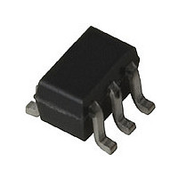
MGA83563TR1 Avago Technologies US Inc., MGA83563TR1 Datasheet - Page 13

MGA83563TR1
Manufacturer Part Number
MGA83563TR1
Description
Manufacturer
Avago Technologies US Inc.
Datasheet
1.MGA83563TR1.pdf
(22 pages)
Specifications of MGA83563TR1
Manufacturer's Type
Power Amplifier
Number Of Channels
1
Supply Current
200@3VmA
Frequency (max)
6GHz
Operating Supply Voltage (typ)
3V
Package Type
SOT-363
Mounting
Surface Mount
Pin Count
6
Lead Free Status / Rohs Status
Not Compliant
13
Input Match
The input return loss without any external matching was
measured as 7.6 dB (2.4:1 VWSR). For many applications
no further matching is necessary. If, however, an im-
proved input match is required, a simple series inductor
is all that will be needed.
Avago’s Touchstone CAD program is again used to extrapo-
late the 2.5 GHz S-parameters in Table 1 and calculate a small
signal *
plotted on the Smith chart as Point A in Figure 25.
-0.2
Figure 25. Initial Small Signal Input Match.
The addition of a 0.15 inch length (actual length on FR-4)
of 50 Ω transmission line rotates Point A around to Point
B on the R = 1 circle of the Smith chart. A series 2.5 nH
inductor (L1) is then all that is required to complete the
match to 50 Ω at Point C.
While the input impedance of the MGA-83563 is some-
what isolated from the nonlinear effects of the saturated
output stage, some empirical optimization of the input
inductor may increase the input return loss still further.
The input is easily fine-tuned under large signal condi-
tions by observing the input return loss while an input
power of +4 dBm is applied to the amplifier. The input
inductor is then “swept” by placing various values of chip
inductors across the gap provided in the 50 Ω line at the
input of the MGA-83563. For this example amplifier, in-
creasing the inductor from the initial small signal value
of 2.5 nH to 2.7 nH was found to provide the best input
match. The final input circuit tuned as for large signal
conditions is shown in Figure 26.
Input
Figure 26. Final Large Signal RF Input Match for the 2.5 GHz Amplifier.
The addition of the 2.7 nH series inductor increased the
large signal input return loss from 7.6 dB (with no match-
ing) to 14.8 dB (1.4:1 VSWR) at 2.5 GHz.
0.2
RF
0.2
-0.5
2.7 nH
0.5
ms
of 0.37 ‘47°. The conjugate of *
C (50 Ω)
Input
RF
0.5
0.17 in.
50 Ω
L1
C
1
-1
1
B
MLIN
B
A (Γ
A
2
ms
MGA-
83563
*)
2
-2
Output
RF
ms
, 0.37 ‘ -47°, is
Completed 2.5 GHz Amplifier
A schematic diagram of the final 2.5 GHz circuit is shown
in Figure 27. All unmarked capacitors are 62 pF.
Input
Figure 27. Schematic Diagram of 2.5 GHz Amplifier.
The completed 2.5 GHz amplifier assembly with all com-
ponents is shown in Figure 28.
Figure 28. Completed 2.5 GHz Amplifier Assembly.
The small signal gain of the completed amplifier was
measured as 22.0 dB at 2.5 GHz. Gain over a frequency
range of 2.0 to 3.0 GHz is shown in Figure 29.
The (small signal) input and output return losses for the
completed amplifier are 14.9 dB and 5.5 dB respectively
at 2.5 GHz. Input and output return loss over the 2.0 to
3.0 GHz frequency range is shown in Figure 30.
Input
RF
Figure 29. Small Signal Gain of the
Completed 2.5 GHz Amplifier.
L1 = 2.7 nH
28
26
24
22
20
18
16
14
2
0.17 in
50 Ω
2.2
L1
FREQUENCY (GHz)
3
83
+3V
2.4
1
6
L2 = 1.5 nH
83
0.08 in
50 Ω
C
RFC =
22 nH
2.6
C2
C2 = 0.9 pF
L2
C
C
2.8
RFC
Output
Output
RF
V
3
d


