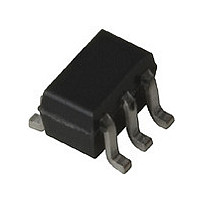
MGA83563TR1 Avago Technologies US Inc., MGA83563TR1 Datasheet - Page 19

MGA83563TR1
Manufacturer Part Number
MGA83563TR1
Description
Manufacturer
Avago Technologies US Inc.
Datasheet
1.MGA83563TR1.pdf
(22 pages)
Specifications of MGA83563TR1
Manufacturer's Type
Power Amplifier
Number Of Channels
1
Supply Current
200@3VmA
Frequency (max)
6GHz
Operating Supply Voltage (typ)
3V
Package Type
SOT-363
Mounting
Surface Mount
Pin Count
6
Lead Free Status / Rohs Status
Not Compliant
19
Appendix —Determination of Interstage Inductor Value.
A methodology is presented here for determining
the value of the interstage inductor, L2 that produces
optimum large signal performance at any frequency.
This is the method used to create the plot of Optimum
L2 vs. Frequency in Figure 19. This procedure is included
as a reference for PCB designs that may differ consider-
ably from the example circuit of Figure 40.
While the method described here covers a wide range of
frequencies for generic applications, the same approach
can be used for a single frequency of interest. Although
the printed circuit board layout of Figure 40 is used here
for demonstration purposes, the same procedure is
equally applicable to the any other circuit board mate-
rial, thickness, or topology.
This is a 2-step process in which the value for L2 for best
small signal performance is first ascertained followed by an
empirical adjustment of L2 to allow for large signal effects.
The first step in this process is to assemble a test circuit
for the MGA-83563 with 50-ohm input and output lines.
This test circuit should use the same printed circuit board
material, thickness, and ground via arrangement for the
MGA-83563 that will be used to the final amplifier circuit.
The connection to Pin 1 should have provision for a chip
inductor that is bypassed to ground. The bypassed side
of the inductor is connected to the supply voltage. The
supply voltage is also connected to the RF Output/V
(Pin 6) by means of an external, wideband bias tee. The
test circuit is shown in Figure 44.
IN
Figure 44. L2 Test Circuit.
Next, the wideband gain response of the test circuit is
observed while substituting various values of chip in-
ductors for L2. For each value of L2, the gain should be
plotted and/or the frequency at which the maximum
gain occurs recorded. Note that the small signal input
and output match provided by the internal matching of
the MGA-83563 is sufficiently close to 50 ohms for most
combinations of L2 and frequencies that further match-
ing would not significantly skew the data. This is a small
signal test and the input power level should be less than
-15 dBm.
Test Circuit
50 Ω
MGA-
83563
L2
50 Ω
BIAS
TEE
OUT
+V
d
d2
Figure 45. Small Signal Gain vs. Frequency for Various Values of L2.
Various values of Toko, Inc.
used for this particular example. An inductance value
of 0.5 nH was used for the case of a short circuit placed
across the gap provided for L2. For use at 5.8 GHz, Pin
1 should be bypassed through the most direct path
(minimum inductance) to ground. Referring to Figure 21,
L2 is not used and a bypass capacitor is placed from Pin 1
directly to the ground pad for Pin 2.
The result of this step is the multiple plot shown in Figure
45 of gain vs. frequency with L2 as a parameter. This plot
is similar to the plot in Table 1, but differs in that the data
in Figure 45 is specific to the designer’s particular PCB
layout. The Table 1 data is a combination of test data
taken in a relatively parasitic-sterile characterization
fixture and computer simulations. The test data in Figure
45 includes the effects of all circuit parasitics, ground
vias, parasitics of the actual chip inductor that will be
used, and also takes into account the length of line and
bypass capacitor used to make the connection to L2 that
will be used in the final circuit.
The value of L2 is then plotted vs. the frequency at which
the gain peak occurred for each value of inductance.
This plot is done as a log plot with a straight-line curve
fit added to smooth the data. This data, shown as Plot
A in Figure 46, then gives the optimum value of L2 for
maximum small signal gain, i.e., linear performance.
The results of the 2.5 GHz and 900 MHz example ampli-
fiers presented in this Application Note were used to
modify Plot A for large signal use. The optimum, large
signal value for L2 at 2.5 GHz was determined to be
1.5 nH, and 12 nH for 900 MHz. These two L2-frequency
points are added to the data plot of Figure 46. A straight
line is drawn through these two points to create Plot B.
25
20
15
10
5
0
0.5 1.0
2.0
FREQUENCY (GHz)
3.0
33
15
6.8
4.0
4.7
2.7
©
1.5
5.0
type LL1608 inductors were
0 nH
6.0


