M50FW040K1 STMicroelectronics, M50FW040K1 Datasheet
M50FW040K1
Specifications of M50FW040K1
Available stocks


Related parts for M50FW040K1


M50FW040K1 Summary of contents
Page 1
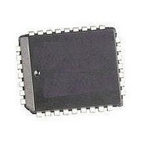
... Program other Blocks during Erase Suspend FOR USE in PC BIOS APPLICATIONS ELECTRONIC SIGNATURE – Manufacturer Code: 20h – Device Code: 2Ch November 2004 4 Mbit (512Kb x8, Uniform Block) 3V Supply Firmware Hub Flash Memory Figure 1. Packages M50FW040 PLCC32 (K) TSOP32 (NB 14mm TSOP40 ( 20mm 1/41 ...
Page 2
M50FW040 TABLE OF CONTENTS FEATURES SUMMARY . . . . . . . . . . . . . . . . . . . . . . . . . . . . . . . . . . ...
Page 3
... Table 4. FWH Bus Read Field Definitions . . . . . . . . . . . . . . . . . . . . . . . . . . . . . . . . . . . . . . . . . . . 12 Figure 7. FWH Bus Read Waveforms Table 5. FWH Bus Write Field Definitions . . . . . . . . . . . . . . . . . . . . . . . . . . . . . . . . . . . . . . . . . . . 13 Figure 8. FWH Bus Write Waveforms COMMAND INTERFACE . . . . . . . . . . . . . . . . . . . . . . . . . . . . . . . . . . . . . . . . . . . . . . . . . . . . . . . . . . . 14 Read Memory Array Command . . . . . . . . . . . . . . . . . . . . . . . . . . . . . . . . . . . . . . . . . . . . . . . . . . . . 14 Read Status Register Command . . . . . . . . . . . . . . . . . . . . . . . . . . . . . . . . . . . . . . . . . . . . . . . . . . . 14 Read Electronic Signature Command . . . . . . . . . . . . . . . . . . . . . . . . . . . . . . . . . . . . . . . . . . . . . . . 14 Program Command . . . . . . . . . . . . . . . . . . . . . . . . . . . . . . . . . . . . . . . . . . . . . . . . . . . . . . . . . . . . . 14 Erase Command . . . . . . . . . . . . . . . . . . . . . . . . . . . . . . . . . . . . . . . . . . . . . . . . . . . . . . . . . . . . . . . 14 Clear Status Register Command . . . . . . . . . . . . . . . . . . . . . . . . . . . . . . . . . . . . . . . . . . . . . . . . . . . 14 Program/Erase Suspend Command ...
Page 4
M50FW040 Device Code Register . . . . . . . . . . . . . . . . . . . . . . . . . . . . . . . . . . . . ...
Page 5
Figure 22.Erase Suspend & Resume Flowchart and Pseudo Code . . . . . . . . . . . . . . . . . . . . . . . . 39 REVISION HISTORY . . . . ...
Page 6
... M50FW040 SUMMARY DESCRIPTION The M50FW040 Mbit (512Kb x8) non-vola- tile memory that can be read, erased and repro- grammed. These operations can be performed using a single low voltage (3.0 to 3.6V) supply. For fast erasing in production lines an optional 12V power supply can be used to reduce the erasing time ...
Page 7
Figure 3. Logic Diagram (A/A Mux Interface A0-A10 RC M50FW040 Figure 4. PLCC Connections A/A Mux DQ0 A/A Mux Note: Pins ...
Page 8
M50FW040 Figure 5. TSOP32 Connections A10 the RB pin is not available for the A/A Mux interface in the ...
Page 9
... High, V After exiting Reset mode, the memory enters Read mode. CPU Reset (INIT). The CPU Reset, INIT, pin is used to Reset the memory when the CPU is reset. It behaves identically to Interface Reset, RP, and the internal Reset line is the logical OR (electrical AND and INIT. ...
Page 10
... Program or Erase operation and it will not accept any additional Program or Erase command except the Program/Erase Sus- pend command. When Ready/Busy is High, V the memory is ready for any Read, Program or Erase operation. Supply Signal Descriptions The Supply Signals are the same for both interfac- es ...
Page 11
... WP). Finally two reset signals (RP and INIT) are available to put the memory into a known state. The data signals, control signal and clock are de- signed to be compatible with PCI electrical specifi- cations ...
Page 12
... Data transfer is two CLK cycles, starting with the least significant O nibble. The FWH Flash Memory drives FWH0-FWH3 to 1111b to indicate a O turnaround cycle. The FWH Flash Memory floats its outputs, the host takes control of N/A FWH0-FWH3. and Write En The Data Inputs/ IL Figure 15 ...
Page 13
... The FWH Flash Memory drives FWH0-FWH3 to 0000b, 0000b O indicating it has received data or a command. The FWH Flash Memory drives FWH0-FWH3 to 1111b, 1111b O indicating a turnaround cycle. 1111b The FWH Flash Memory floats its outputs and the host takes N/A (float) control of FWH0-FWH3. IDSEL ADDR MSIZE DATA 1 ...
Page 14
... Table 6. Program Command. The Program command can be used to program a value to one address in the memory array at a time. Two Bus Write opera- tions are required to issue the command; the sec- ond Bus Write cycle latches the address and data in the internal state machine and starts the Pro- gram/Erase Controller ...
Page 15
... Program/Erase Controller has paused. After the Program/Erase Controller has paused, the memory will continue to output the Status Reg- ister until another command is issued. During the polling period between issuing the Pro- gram/Erase Suspend command and the Program/ Erase Controller pausing it is possible for the op- eration to complete ...
Page 16
... Note: X Don’t Care, PA Program Address, PD Program Data, BA Any address in the Block. Read Memory Array. After a Read Memory Array command, read the memory as normal until another command is issued. Read Status Register. After a Read Status Register command, read the Status Register as normal until another command is issued. ...
Page 17
... The Program Status bit should be read once the Program/Erase Controller Status bit is ‘1’ (Program/Erase Controller inactive). When the Program Status bit is ‘0’ the memory has successfully verified that the byte has pro- grammed correctly; when the Program Status bit is ‘ ...
Page 18
... Program/Erase Controller Status bit is ‘1’ (Program/Erase Control- ler inactive); after a Program/Erase Suspend com- mand is issued the memory may still complete the operation rather than entering the Suspend mode. When the Program Suspend Status bit is ‘0’ the Program/Erase Controller is active or has complet- ed its operation ...
Page 19
... Manufacturer Code Register Reading the Manufacturer Code Register returns the manufacturer code for the memory. The man- ufacturer code for STMicroelectronics is 20h. This register is read-only and writing to it has no effect. Device Code Register Reading the Device Code Register returns the de- vice code for the memory, 2Ch ...
Page 20
... Read-Lock ‘0’ Bus read operations in this Block return the Memory Array contents. (Default value). Changes to the Read-Lock bit and the Write-Lock bit cannot be performed. Once a ‘1’ is ‘1’ written to the Lock-Down bit it cannot be cleared to ‘0’; the bit is always reset to ‘0’ following ...
Page 21
PROGRAM AND ERASE TIMES The Program and Erase times are shown in 12. Table 12. Program and Erase Times Parameter Byte Program Block Program Block Erase Program/Erase Suspend to Program pause(2) Program/Erase Suspend to Block Erase pause Note ...
Page 22
... Minimum Voltage may undershoot to –2V and for less than 20ns during transitions. Maximum Voltage may overshoot to V and for less than 20ns during transitions. 22/41 plied. Exposure to Absolute Maximum Rating con- ditions for extended periods may affect device reliability. Refer also to the STMicroelectronics SURE Program and other relevant quality docu- ments. Parameter Min ...
Page 23
DC AND AC PARAMETERS This section summarizes the operating measure- ment conditions, and the DC and AC characteris- tics of the device. The parameters in the DC and AC characteristics Tables that follow, are derived from tests performed under the ...
Page 24
M50FW040 Figure 10. A/A Mux Interface AC Testing Input Output Waveform Table 17. Impedance Symbol Parameter (1) Input Capacitance C IN (1) Clock Capacitance C CLK Recommended Pin (2) L PIN Inductance Note: 1. Sampled only, not 100% tested. 2. ...
Page 25
Table 18. DC Characteristics Symbol Parameter V Input High Voltage IH V Input Low Voltage IL V (INIT) INIT Input High Voltage IH V (INIT) INIT Input Low Voltage IL (2) Input Leakage Current I LI IC, IDx Input Leakage ...
Page 26
M50FW040 Figure 11. FWH Interface Clock Waveform Table 19. FWH Interface Clock Characteristics Symbol Parameter (1) t CLK Cycle Time CYC t CLK High Time ...
Page 27
Figure 12. FWH Interface AC Signal Timing Waveforms CLK tCHQV FWH0-FWH3 VALID OUTPUT DATA Table 20. FWH Interface AC Signal Timing Characteristics PCI Symbol Symbol t t CLK to Data Out CHQV val CLK to Active ( ...
Page 28
M50FW040 Figure 13. Reset AC Waveforms RP, INIT W, G, FWH4 RB Table 21. Reset AC Characteristics Symbol Parameter INIT Reset Pulse Width PLPH INIT Low to Reset PLRH RP or INIT Slew Rate ...
Page 29
Figure 14. A/A Mux Interface Read AC Waveforms A0-A10 ROW ADDR VALID tAVCL tCLAX RC G DQ0-DQ7 W tPHAV RP Table 22. A/A Mux Interface Read AC Characteristics Symbol Parameter t Read Cycle Time AVAV t Row Address Valid to ...
Page 30
M50FW040 Figure 15. A/A Mux Interface Write AC Waveforms Write erase or program setup A0-A10 R1 tCLAX tAVCL RC tWHWL tWLWH DQ0-DQ7 Table 23. A/A Mux Interface Write AC Characteristics Symbol Parameter t Write Enable ...
Page 31
PACKAGE MECHANICAL Figure 16. PLCC32 – 32 pin Rectangular Plastic Leaded Chip Carrier, Package Outline Note: Drawing is not to scale 0.51 (.020) 1.14 (.045) R M50FW040 A1 A2 ...
Page 32
M50FW040 Table 24. PLCC32 – 32 pin Rectangular Plastic Leaded Chip Carrier, Package Mechanical Data Symbol Typ 7. 10. 0.89 N 32/41 ...
Page 33
Figure 17. TSOP32 – 32 lead Plastic Thin Small Outline, 8x14 mm, Package Outline 1 N/2 TSOP-a Note: Drawing is not to scale. Table 25. TSOP32 – 32 lead Plastic Thin Small Outline, 8x14 mm, Package Mechanical Data Symbol Typ ...
Page 34
M50FW040 Figure 18. TSOP40 – 40 lead Plastic Thin Small Outline, 10x20 mm, Package Outline 1 N/2 TSOP-a Note: Drawing is not to scale. Table 26. TSOP40 – 40 lead Plastic Thin Small Outline, 10x20 mm, Package Mechanical Data Symbol ...
Page 35
... Standard SnPb plating G = Lead-Free, RoHS compliant, Sb2O3-free and TBBA-free Devices are shipped from the factory with the memory content bits erased to ’1’. For a list of available options (Speed, Package, etc.) or for further information on any aspect of this device, please contact the ST Sales Office nearest to you. ...
Page 36
... Error) can be made after each Program operation by PP Program command: – write 40h or 10h – write Address & Data (memory enters read status state after the Program command) do: –read Status Register if Program/Erase Suspend command given execute suspend program loop ...
Page 37
Figure 20. Program Suspend & Resume Flowchart and Pseudo Code Start Write B0h Write 70h Read Status Register YES YES Write a read Command Read data from another address Write D0h Program Continues NO ...
Page 38
... Erase Error (1) NO Erase to Protected Block Error (1) Erase command: – write 20h – write Block Address & D0h (memory enters read Status Register after the Erase command) do: – read Status Register – if Program/Erase Suspend command given execute suspend erase loop while invalid error: – ...
Page 39
Figure 22. Erase Suspend & Resume Flowchart and Pseudo Code Start Write B0h Write 70h Read Status Register YES YES Read data from another block or Program Write D0h Erase Continues NO NO Erase ...
Page 40
M50FW040 REVISION HISTORY Table 28. Document Revision History Date Version September 2000 -01 04-Oct-2000 -02 11-Apr-01 -03 06-Jul-2001 -04 12-Mar-2002 -05 09-Jul-2004 6.0 12-Jul-2004 7.0 10-Nov-2004 8.0 40/41 Revision Details First Issue DC Characteristics: I changed CC4 Document type: from ...
Page 41
... No license is granted by implication or otherwise under any patent or patent rights of STMicroelectronics. Specifications mentioned in this publication are subject to change without notice. This publication supersedes and replaces all information previously supplied. STMicroelectronics products are not authorized for use as critical components in life support devices or systems without express written approval of STMicroelectronics ...