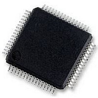
AD7609BSTZ Analog Devices Inc, AD7609BSTZ Datasheet - Page 21

AD7609BSTZ
Manufacturer Part Number
AD7609BSTZ
Description
58T8900
Manufacturer
Analog Devices Inc
Datasheet
1.AD7609BSTZ.pdf
(36 pages)
Specifications of AD7609BSTZ
Resolution (bits)
18bit
Sampling Rate
250kSPS
Input Channel Type
Differential
Data Interface
Serial, SPI
Supply Voltage Range - Analog
4.75V To 5.25V
Rohs Compliant
Yes
Available stocks
Company
Part Number
Manufacturer
Quantity
Price
Company:
Part Number:
AD7609BSTZ
Manufacturer:
ADI
Quantity:
433
Company:
Part Number:
AD7609BSTZ
Manufacturer:
ADI
Quantity:
250
Company:
Part Number:
AD7609BSTZ
Manufacturer:
Analog Devices Inc
Quantity:
10 000
Part Number:
AD7609BSTZ
Manufacturer:
ADI/亚德诺
Quantity:
20 000
Company:
Part Number:
AD7609BSTZ-RL
Manufacturer:
Analog Devices Inc
Quantity:
10 000
THEORY OF OPERATION
CONVERTER DETAILS
The
speed, low power, charge redistribution successive approxima-
tion analog-to-digital converter (ADC) and allows the
simultaneous sampling of eight true differential analog input
channels. The analog inputs on the
bipolar input signals. The RANGE pin is used to select either
±10 V or ±5 V as the input range. The
a single 5 V supply.
The
scaling amplifiers, a second-order antialiasing filter, track-and-
hold amplifiers, an on-chip reference, reference buffers, a high
speed ADC, a digital filter, and high speed parallel and serial
interfaces. Sampling on the
CONVST x signals.
ANALOG INPUT
Analog Input Ranges
The
level on the RANGE pin determines the analog input range of
all analog input channels. If this pin is tied to a logic high, the
analog input range is ±10 V for all channels. If this pin is tied
to a logic low, the analog input range is ±5 V for all channels.
A logic change on this pin has an immediate effect on the
analog input range; however, there is a settling time of 80 μs
typically, in addition to the normal acquisition time
requirement. The recommended practice is to hardwire the
RANGE pin according to the desired input range for the system
signals.
Analog Input Impedance
The analog input impedance of the
fixed input impedance and does not vary with the
pling frequency. This high analog input impedance eliminates
the need for a driver amplifier in front of the
for direct connection to the source or sensor. With the need for
a driver amplifier eliminated, bipolar supplies can be removed
from the signal chain, which are often a source of noise in a system.
AD7609
AD7609
AD7609
is a data acquisition system that employs a high
contains input clamp protection, input signal
can handle true bipolar input voltages. The logic
AD7609
AD7609
AD7609
is controlled using
AD7609
can accept true
is 1 MΩ. This is a
AD7609
operates from
AD7609
allowing
sam-
Rev. 0 | Page 21 of 36
Analog Input Clamp Protection
Figure 32 shows the analog input structure of the AD7609.
Each
Despite a single 5 V supply operation, this analog input clamp
protection allows for an input over voltage up to ±16.5 V.
Figure 33 shows the current vs. voltage characteristic of the
clamp circuit. For input voltages up to ±16.5 V, no current flows
in the clamp circuit. For input voltages above ±16.5 V, the
AD7609
to ±16.5 V. A series resister should be placed on the analog
input channels to limit the current to ±10 mA for input voltages
above ±16.5 V. In an application where there is a series resistance
on an analog input channel, VINx+, a corresponding resistance
is required on the VINx− channel (see Figure 34). If there is no
corresponding resister on the Vx− channel, this results in an
offset error on that channel. It is recommended that the input
overvoltage clamp protection circuitry be used to protect the
AD7609
mended to leave the
protection circuitry is active (in normal or power-down
conditions) for extended periods because this may degrade the
bipolar zero code error performance of the AD7609.
+10V
–10V
+10V
–10V
AD7609
Vx+
Vx–
–10
–20
–30
–40
–50
30
20
10
Figure 34. Input Resistance Matching on the Analog Input
0
–20
clamp circuitry turns on and clamps the analog input
against transient overvoltage events. It is not recom-
AV
T
A
CC
= 25°C
CLAMP
CLAMP
analog input contains clamp protection circuitry.
, V
–15
Figure 33. Input Protection Clamp Profile
DRIVE
Figure 32. Analog Input Circuitry
R
R
C
AD7609
–10
1MΩ
1MΩ
= 5V
VINx+
VINx–
SOURCE VOLTAGE (V)
–5
R
R
FB
FB
in a condition where the clamp
AD7609
CLAMP
CLAMP
0
SECOND-
ORDER
LPF
5
1MΩ
1MΩ
10
R
R
FB
FB
15
AD7609
20


