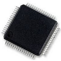
AD7609BSTZ Analog Devices Inc, AD7609BSTZ Datasheet - Page 22

AD7609BSTZ
Manufacturer Part Number
AD7609BSTZ
Description
58T8900
Manufacturer
Analog Devices Inc
Datasheet
1.AD7609BSTZ.pdf
(36 pages)
Specifications of AD7609BSTZ
Resolution (bits)
18bit
Sampling Rate
250kSPS
Input Channel Type
Differential
Data Interface
Serial, SPI
Supply Voltage Range - Analog
4.75V To 5.25V
Rohs Compliant
Yes
Available stocks
Company
Part Number
Manufacturer
Quantity
Price
Company:
Part Number:
AD7609BSTZ
Manufacturer:
ADI
Quantity:
433
Company:
Part Number:
AD7609BSTZ
Manufacturer:
ADI
Quantity:
250
Company:
Part Number:
AD7609BSTZ
Manufacturer:
Analog Devices Inc
Quantity:
10 000
Part Number:
AD7609BSTZ
Manufacturer:
ADI/亚德诺
Quantity:
20 000
Company:
Part Number:
AD7609BSTZ-RL
Manufacturer:
Analog Devices Inc
Quantity:
10 000
AD7609
Analog Input Antialiasing Filter
An analog antialiasing filter is also provided on the AD7609.
The filter is a second-order Butterworth. Figure 35 and
Figure 36 show the frequency and phase response respectively
of the analog antialiasing filter. In the ±5 V range, the −3 dB
frequency is typically 23 kHz. In the ±10 V range, the −3 dB
frequency is typically 32 kHz.
Track-and-Hold Amplifiers
The track-and-hold amplifiers on the
accurately acquire an input sine wave of full-scale amplitude
to 18-bit resolution. The track-and-hold amplifiers sample
their respective inputs simultaneously on the rising edge of
CONVST x. The aperture time for track-and-hold (that is, the
delay time between the external CONVST x signal and the
track-and-hold actually going into hold) is well matched, by design,
across all eight track-and-holds on one device and from device
to device. This matching allows more than one
to be sampled simultaneously in a system.
The end of the conversion process across all eight channels is
indicated by the falling edge of BUSY; and it is at this point that the
track-and-holds return to track mode and the acquisition time
for the next set of conversions begins.
–10
–15
–20
–25
–30
–35
–40
–5
14
13
12
11
10
0
9
8
7
6
5
4
3
2
1
0
100
Figure 35. Analog Antialiasing Filter Frequency Response
10
Figure 36. Analog Antialiasing Filter Phase Response
AV
f
T
±10V RANGE
SAMPLE
±5V RANGE
A
10V
5V
CC
= 25°C
, V
TEMP
–40°C 13,354Hz 33,520Hz
–40°C 10,303Hz 24,365Hz
25°C 12,769Hz 32,397Hz
85°C 12,427Hz 31,177Hz
25°C
85°C
DRIVE
= 200kSPS
9619Hz 23,389Hz
9326Hz 22,607Hz
= 5V
0.1dB
INPUT FREQUENCY (Hz)
1k
1k
FREQUENCY (Hz)
3dB
AD7609
10k
10k
5V DIFF
allow the ADC to
AD7609
10V DIFF
100k
100k
device
Rev. 0 | Page 22 of 36
The conversion clock for the part is internally generated, and
the conversion time for all channels is 4 μs on the AD7609. The
BUSY signal returns low after all eight conversions to indicate the
end of the conversion process. On the falling edge of BUSY, the
track-and-hold amplifiers return to track mode. New data can
be read from the output register via the parallel, or serial
interface after BUSY goes low; or, alternatively, data from the
previous conversion can be read while BUSY is high. Reading data
from the
effect on performance and allows a faster throughput to be
achieved. With a V
when reading during a conversion.
ADC TRANSFER FUNCTION
The output coding of the
designed code transitions occur midway between successive
integer LSB values, that is, 1/2 LSB, 3/2 LSB. The LSB size is
FSR/262,144 for the AD7609. The FSR for the
for the ±10 V range and 20 V for the ±5 V range. The ideal
transfer characteristic for the
The LSB size is dependent on the analog input range selected
(see Table 7).
Table 7. Output Codes and Ideal Input Values
Description
FSR − 0.5 LSB
Midscale + 1 LSB
Midscale
Midscale – 1 LSB
−FSR + 1 LSB
−FSR
AD7609
011...111
011...110
000...001
000...000
111...111
100...010
100...001
100...000
Figure 37.
–FS + 1/2LSB
while a conversion is in progress has little
DRIVE
±10V CODE =
Analog Input
(V+ − (V−)
10 V Range
+19.99992 V
+152.58 μV
0 V
−152.58 μV
−19.99984 V
−20 V
±5V CODE =
AD7609
> 3.3 V, the SNR is reduced by ~1.5 dB
0V – 1LSB +FS – 3/2LSB
AD7609
ANALOG INPUT
AD7609
V+ ± (V–)
V+ ± (V–)
Transfer Characteristic
10V
5V
is twos complement. The
Analog
Input
V+ − (V−)
5 V Range
9.999961 V
0 V
−76 μV
−9.99992 V
−10 V
76 μV
× 131,072 ×
× 131,072 ×
is shown in Figure 37.
LSB =
+FSR – (–FSR)
2.5V
2.5V
AD7609
REF
REF
2
18
Digital
Output
Code (Hex)
0x1FFFF
0x00001
0x00000
0x3FFFF
0x20001
0x20000
is 40 V


