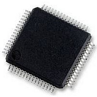
AD7609BSTZ Analog Devices Inc, AD7609BSTZ Datasheet - Page 28

AD7609BSTZ
Manufacturer Part Number
AD7609BSTZ
Description
58T8900
Manufacturer
Analog Devices Inc
Datasheet
1.AD7609BSTZ.pdf
(36 pages)
Specifications of AD7609BSTZ
Resolution (bits)
18bit
Sampling Rate
250kSPS
Input Channel Type
Differential
Data Interface
Serial, SPI
Supply Voltage Range - Analog
4.75V To 5.25V
Rohs Compliant
Yes
Available stocks
Company
Part Number
Manufacturer
Quantity
Price
Company:
Part Number:
AD7609BSTZ
Manufacturer:
ADI
Quantity:
433
Company:
Part Number:
AD7609BSTZ
Manufacturer:
ADI
Quantity:
250
Company:
Part Number:
AD7609BSTZ
Manufacturer:
Analog Devices Inc
Quantity:
10 000
Part Number:
AD7609BSTZ
Manufacturer:
ADI/亚德诺
Quantity:
20 000
Company:
Part Number:
AD7609BSTZ-RL
Manufacturer:
Analog Devices Inc
Quantity:
10 000
AD7609
DIGITAL FILTER
The
is a first-order sinc filter. This digital filter should be used in
applications where slower throughput rates are used or where
higher signal-to-noise ratio or dynamic range is desirable. The
oversampling ratio of the digital filter is controlled using the
oversampling pins, OS [2:0] (see Table 9). OS 2 is the MSB
control bit and OS 0 is the LSB control bit. Table 9 provides
the oversampling bit decoding to select the different oversample
rates. The OS pins are latched on the falling edge of BUSY.
This sets the oversampling rate for the next conversion (see
Figure 45). In addition to the oversampling function, the output
result is decimated to 18-bit resolution.
If the OS pins are set to select an OS ratio of 8, the next
CONVST x rising edge takes the first sample for each channel
and the remaining seven samples for all channels are taken with
an internally generated sampling signal. These samples are then
averaged to yield an improvement in SNR performance. Table 9
shows typical SNR performance for both the ±10 V and the
±5 V ranges. As Table 9 indicates, there is an improvement in
SNR as the OS ratio increases. As the OS ratio increases, the
3 dB frequency is reduced and the allowed sampling frequency
is also reduced. In an application where the required sampling
frequency is 10 kSPS, an OS ratio of up to 16 can be used. In
this case, the application sees an improvement in SNR but the
input −3 dB bandwidth is limited to ~6 kHz.
Table 9. Oversampling Bit Decoding (100 Hz Input Signal)
OS
[2:0]
000
001
010
011
100
101
110
111
AD7609
OS
Ratio
No OS
2
4
8
16
32
64
Invalid
contains an optional digital filter. This digital filter
SNR ±5 V Range
(dB)
90.8
93.3
95.5
98
100.6
101.8
102.7
CONVST A,
CONVST B
BUSY
OS x
SNR ±10 V Range
(dB)
91.5
93.9
96.4
98.9
101
102
102.9
t
OS_SETUP
CONVERSION N
Figure 45. OS Pin Timing
OVERSAMPLE RATE
LATCHED FOR CONVERSION N + 1
Rev. 0 | Page 28 of 36
−3 dB BW 5 V Range
(kHz)
22
22
18.5
11.9
6
3
1.5
t
OS_HOLD
The CONVST A and CONVST B pins must be tied/driven
together when oversampling is turned on. When the over-
sampling function is turned on, the BUSY high time for the
conversion process extends. The actual BUSY high time
depends on the oversampling rate selected; the higher the
oversampling rate, the longer the BUSY high, or total
conversion time, see Table 9.
Figure 46 shows that the conversion time extends as the over-
sampling rate is increased, and the BUSY signal lengthens for the
different oversampling rates. For example, a sampling frequency
of 10 kSPS yields a cycle time of 100 μs. Figure 46 shows OS × 2
and OS × 4; for a 10 kSPS example, there is adequate cycle time
to further increase the oversampling rate and yield greater
improvements in SNR performance. In an application where
the initial sampling or throughput rate is at 200 kSPS, for
example, and oversampling is turned on, the throughput rate
must be reduced to accommodate the longer conversion time
and to allow for the read. To achieve the fastest throughput
rate possible when oversampling is turned on, the read can be
performed during the BUSY high time. The falling edge of BUSY
is used to update the output data registers with the new conver-
sion data; therefore, the reading of conversion data should not
occur on this edge. Figure 47 to Figure 53 illustrate the effect of
oversampling on the code spread in a dc histogram plot. As the
oversample rate is increased, the spread of codes is reduced. (In
Figure 47 to Figure 53, AV
rate was scaled with OS ratio.)
−3 dB BW 10 V
Range (kHz)
33
28.9
21.5
12
6
3
1.5
CONVERSION N + 1
CC
= V
DRIVE
Maximum Throughput
CONVST x Frequency (kHz)
200
100
50
25
12.5
6.25
3.125
= 5 V and the sampling


