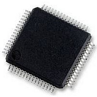
AD7609BSTZ Analog Devices Inc, AD7609BSTZ Datasheet - Page 32

AD7609BSTZ
Manufacturer Part Number
AD7609BSTZ
Description
58T8900
Manufacturer
Analog Devices Inc
Datasheet
1.AD7609BSTZ.pdf
(36 pages)
Specifications of AD7609BSTZ
Resolution (bits)
18bit
Sampling Rate
250kSPS
Input Channel Type
Differential
Data Interface
Serial, SPI
Supply Voltage Range - Analog
4.75V To 5.25V
Rohs Compliant
Yes
Available stocks
Company
Part Number
Manufacturer
Quantity
Price
Company:
Part Number:
AD7609BSTZ
Manufacturer:
ADI
Quantity:
433
Company:
Part Number:
AD7609BSTZ
Manufacturer:
ADI
Quantity:
250
Company:
Part Number:
AD7609BSTZ
Manufacturer:
Analog Devices Inc
Quantity:
10 000
Part Number:
AD7609BSTZ
Manufacturer:
ADI/亚德诺
Quantity:
20 000
Company:
Part Number:
AD7609BSTZ-RL
Manufacturer:
Analog Devices Inc
Quantity:
10 000
AD7609
LAYOUT GUIDELINES
The printed circuit board that houses the
AD7609
should be
designed so that the analog and digital sections are separated
and confined to different areas of the board.
Use at least one ground plane. It can be common or split
between the digital and analog sections. In the case of the split
plane, the digital and analog ground planes should be joined in
only one place, preferably as close as possible to the AD7609.
If the
AD7609
is in a system where multiple devices require
analog-to-digital ground connections, the connection should
still be made at only one point, a star ground point, which
should be established as close as possible to the AD7609. Good
connections should be made to the ground plane. Avoid sharing
one connection for multiple ground pins. Individual vias or
Figure 60. Top Layer Decoupling REFIN/REFOUT, REFCAPA, REFCAPB, and
multiple vias to the ground plane should be used for each
REGCAP Pins
ground pin.
Avoid running digital lines under the devices because doing
so couples noise onto the die. Allow the analog ground plane
to run under the
AD7609
to avoid noise coupling. Shield fast-
switching signals like CONVST A, CONVST B, or clocks with
digital ground to avoid radiating noise to other sections of the
board, and they should never run near analog signal paths.
Avoid crossover of digital and analog signals. Run traces on
layers in close proximity on the board at right angles to each
other to reduce the effect of feedthrough through the board.
The power supply lines to the AV
and V
pins on the
CC
DRIVE
AD7609
should use as large a trace as possible to provide low
impedance paths and reduce the effect of glitches on the power
supply lines. Where possible, use supply planes. Good connec-
tions should be made between the
AD7609
supply pins and the
power tracks on the board; this should involve the use of a single
Figure 61. Bottom Layer Decoupling
via or multiple vias for each supply pin.
Good decoupling is also important to lower the supply imped-
ance presented to the
AD7609
and to reduce the magnitude of
the supply spikes. Place the decoupling capacitors close to,
ideally right up against, these pins and their corresponding
ground pins. Place the decoupling capacitors for the REFIN/
REFOUT pin and the REFCAPA and REFCAPB pins as close as
possible to their respective
AD7609
pins. Where possible, they
should be placed on the same side of the board as the
AD7609
device. Figure 60 shows the recommended decoupling on the
top layer of the
AD7609
board. Figure 61 shows bottom layer
decoupling. Bottom layer decoupling is for the four AV
pins
CC
and the V
pin.
DRIVE
Rev. 0 | Page 32 of 36


