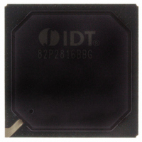
IDT82P2816BBG IDT, Integrated Device Technology Inc, IDT82P2816BBG Datasheet - Page 29

IDT82P2816BBG
Manufacturer Part Number
IDT82P2816BBG
Description
IC LINE INTERFACE UNIT 416-PBGA
Manufacturer
IDT, Integrated Device Technology Inc
Datasheet
1.IDT82P2816BBG.pdf
(146 pages)
Specifications of IDT82P2816BBG
Function
Line Interface Unit (LIU)
Interface
E1, J1, T1
Number Of Circuits
1
Voltage - Supply
1.8V, 3.3V
Operating Temperature
-40°C ~ 85°C
Mounting Type
Surface Mount
Package / Case
*
Includes
Defect and Alarm Detection, Driver Over-Current Detection and Protection, LLOS Detection, PRBSARB / IB Detection and Generation
Number Of Transceivers
1
Screening Level
Industrial
Mounting
Surface Mount
Operating Temperature (min)
-40C
Operating Temperature (max)
85C
Lead Free Status / RoHS Status
Lead free / RoHS Compliant
Current - Supply
-
Power (watts)
-
Lead Free Status / RoHS Status
Compliant, Lead free / RoHS Compliant
Other names
800-1702
82P2816BBG
82P2816BBG
Available stocks
Company
Part Number
Manufacturer
Quantity
Price
Company:
Part Number:
IDT82P2816BBG
Manufacturer:
IDT Integrated Device Technolo
Quantity:
135
Company:
Part Number:
IDT82P2816BBG
Manufacturer:
IDT
Quantity:
70
Company:
Part Number:
IDT82P2816BBG
Manufacturer:
IDT, Integrated Device Technology Inc
Quantity:
10 000
3.2.7
sponding receiver.
RTIPn/RRINGn pins are forced to High-Z state. The pins on receive
system interface (including RDn/RDPn, RDNn/RMFn, RCLKn/RMFn)
will be in High-Z state if the RHZ bit (b6, RCF0,...) is ‘1’ or in low level if
the RHZ bit (b6, RCF0,...) is ‘0’.
receiver to achieve steady state, i.e., to return to the previous configura-
tion and performance.
Functional Description
IDT82P2816
Set the R_OFF bit (b5, RCF0,...) to ‘1’ will power down the corre-
In this way, the corresponding receive circuit is turned off and the
After clearing the R_OFF bit (b5, RCF0,...), it will take 1 ms for the
RECEIVER POWER DOWN
16(+1) CHANNEL HIGH-DENSITY T1/E1/J1 LINE INTERFACE UNIT
29
3.3
3.3.1
Single Rail NRZ Format mode, Dual Rail NRZ Format mode and Dual
Rail RZ Format mode, as selected by the T_MD[1:0] bits (b1~0,
TCF1,...).
mode) or 2.048 MHz (in E1 mode) clock is input on TCLKn, the transmit
system interface is in Single Rail NRZ Format mode. In this mode, the
data is encoded and sampled on the active edge of TCLKn. TMFn is
updated on the active edge of TCLKn and can be selected to indicate
PRBS/ARB, SAIS, TOC, TLOS or SEXZ. Refer to Section 3.5.7.2 TMFn
Indication for the description of TMFn.
(in T1/J1 mode) or 2.048 MHz (in E1 mode) clock is input on TCLKn, the
transmit system interface is in Dual Rail NRZ Format mode. In this
mode, the data is pre-encoded and sampled on the active edge of
TCLKn.
clock is input, the transmit system interface is in Dual Rail RZ Format
mode. In this mode, the data is pre-encoded. TMFn can be selected to
indicate PRBS/ARB, SAIS, TOC, TLOS, SEXZ, SBPV, SEXZ + SBPV or
SLOS. Refer to Section 3.5.7.2 TMFn Indication for the description of
TMFn. The Tx Clock Recovery block is used to recover the clock signal
from the data input on TDPn and TDNn. Refer to Section 3.3.2 Tx Clock
Recovery.
system interface.
The data from the system side is input to the device in three modes:
If data is input on TDn in NRZ format and a 1.544 MHz (in T1/J1
If data is input on TDPn and TDNn in NRZ format and a 1.544 MHz
If data is input on TDPn and TDNn in RZ format and no transmit
Table-4 summarizes the multiplex pin used in different transmit
TRANSMIT PATH
TRANSMIT SYSTEM INTERFACE
February 6, 2009


