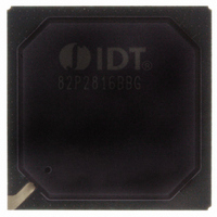
IDT82P2816BBG IDT, Integrated Device Technology Inc, IDT82P2816BBG Datasheet - Page 87

IDT82P2816BBG
Manufacturer Part Number
IDT82P2816BBG
Description
IC LINE INTERFACE UNIT 416-PBGA
Manufacturer
IDT, Integrated Device Technology Inc
Datasheet
1.IDT82P2816BBG.pdf
(146 pages)
Specifications of IDT82P2816BBG
Function
Line Interface Unit (LIU)
Interface
E1, J1, T1
Number Of Circuits
1
Voltage - Supply
1.8V, 3.3V
Operating Temperature
-40°C ~ 85°C
Mounting Type
Surface Mount
Package / Case
*
Includes
Defect and Alarm Detection, Driver Over-Current Detection and Protection, LLOS Detection, PRBSARB / IB Detection and Generation
Number Of Transceivers
1
Screening Level
Industrial
Mounting
Surface Mount
Operating Temperature (min)
-40C
Operating Temperature (max)
85C
Lead Free Status / RoHS Status
Lead free / RoHS Compliant
Current - Supply
-
Power (watts)
-
Lead Free Status / RoHS Status
Compliant, Lead free / RoHS Compliant
Other names
800-1702
82P2816BBG
82P2816BBG
Available stocks
Company
Part Number
Manufacturer
Quantity
Price
Company:
Part Number:
IDT82P2816BBG
Manufacturer:
IDT Integrated Device Technolo
Quantity:
135
Company:
Part Number:
IDT82P2816BBG
Manufacturer:
IDT
Quantity:
70
Company:
Part Number:
IDT82P2816BBG
Manufacturer:
IDT, Integrated Device Technology Inc
Quantity:
10 000
SCAL - Amplitude Scaling Control Register
AWG0 - Arbitrary Waveform Generation Control Register 0
Address: 007H, 047H, 087H, 0C7H, 107H, 147H, 187H, 1C7H, (CH1~CH8)
Type: Read / Write
Default Value: 36H
Address: 008H, 048H, 088H, 0C8H, 108H, 148H, 188H, 1C8H, (CH1~CH8)
Type: Read / Write
Default Value: 00H
Programming Information
IDT82P2816
7 - 6
5 - 0
4 - 0
Bit
Bit
7
6
5
208H, 248H, 288H, 2C8H, 308H, 348H, 388H, 3C8H, (CH9~CH16)
7C8H (CH0)
207H, 247H, 287H, 2C7H, 307H, 347H, 387H, 3C7H, (CH9~CH16)
7C7H (CH0)
7
7
-
-
SAMP[4:0]
SCAL[5:0]
DONE
Name
Name
RW
-
-
DONE
6
6
-
Reserved.
This bit is valid only when the user-programmable arbitrary waveform is enabled (i.e., the PULS[3:0] bits (b3~0, PULS,...) are set
to ‘1XXX’). This bit determines whether to enable the data writing/reading from RAM.
0: Disable. (default)
1: Enable.
This bit is valid only when the user-programmable arbitrary waveform is enabled (i.e., the PULS[3:0] bits (b3~0, PULS,...) are set
to ‘1XXX’). This bit determines read/write direction.
0: Write data to RAM. (default)
1: Read data from RAM.
These bits are valid only when the user-programmable arbitrary waveform is enabled (i.e., the PULS[3:0] bits (b3~0, PULS,...)
are set to ‘1XXX’). These bits specify the RAM sample address.
00000: The RAM sample address is 0. (default)
00001: The RAM sample address is 1.
00010: The RAM sample address is 2.
......
10001: The RAM sample address is 17.
10010: The RAM sample address is 18.
10011 ~ 11111: The RAM sample address is 19.
Reserved.
These bits specify a scaling factor to be applied to the amplitude of the waveform to be transmitted.
In T1/J1 mode, the standard value is ‘110110’ for the waveform amplitude. If necessary, increasing or decreasing by ‘1’ from the
standard value will result in 2% scaling up or down against the waveform amplitude. The scale range is from +20% to -100%.
In E1 mode, the standard value is ‘100001’ for the waveform amplitude. If necessary, increasing or decreasing by ‘1’ from the
standard value will result in 3% scaling up or down against the waveform amplitude. The scale range is from +100% to -100%.
Note: The default value for SCAL[5:0] is ‘110110’ which is the T1/J1 standard value. Therefore, if E1 mode is used, ‘100001’
should be written to these bits to indicate the E1 standard value.
SCAL5
RW
5
5
SAMP4
SCAL4
4
4
16(+1) CHANNEL HIGH-DENSITY T1/E1/J1 LINE INTERFACE UNIT
87
SAMP3
SCAL3
3
3
Description
Description
SCAL2
SAMP2
2
2
SCAL1
SAMP1
1
1
February 6, 2009
SCAL0
SAMP0
0
0


