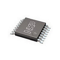
PCA9546PW/G,118 NXP Semiconductors, PCA9546PW/G,118 Datasheet - Page 12

PCA9546PW/G,118
Manufacturer Part Number
PCA9546PW/G,118
Description
Manufacturer
NXP Semiconductors
Datasheet
1.PCA9546PWG118.pdf
(17 pages)
Specifications of PCA9546PW/G,118
Logical Function
I2C Multiplexer
Configuration
1 x 4:1
Number Of Inputs
4
Number Of Outputs
1
Operating Supply Voltage (typ)
2.5/3.3/5V
Operating Supply Voltage (min)
2.3V
Operating Supply Voltage (max)
5.5V
Power Dissipation
400mW
Operating Temp Range
-40C to 85C
Operating Temperature Classification
Industrial
Mounting
Surface Mount
Pin Count
16
Package Type
TSSOP
Lead Free Status / Rohs Status
Compliant
1. Pass gate propagation delay is calculated from the 20
2. A device must internally provide a hold time of at least 300 ns for the SDA signal (referred to the V
3. C
Philips Semiconductors
AC CHARACTERISTICS
NOTES:
2004 Sep 30
SYMBOL
t
t
t
4-channel I
t
t
VD:DATH
t
RESET
t
t
t
VD:DATL
REC:STA
t
VD:ACK
the undefined region of the falling edge of SCL.
HD;STA
SU;STA
SU;STO
HD;DAT
SU;DAT
t
WL(rst)
t
f
t
HIGH
LOW
SCL
BUF
t
b
t
C
t
t
t
SP
pd
rst
R
F
= total capacitance of one bus line in pF.
b
SDA
SCL
Propagation delay from SDA to SD
SCL clock frequency
Bus free time between a STOP and START condition
Hold time (repeated) START condition
After this period, the first clock pulse is generated
LOW period of the SCL clock
HIGH period of the SCL clock
Set-up time for a repeated START condition
Set-up time for STOP condition
Data hold time
Data set-up time
Rise time of both SDA and SCL signals
Fall time of both SDA and SCL signals
Capacitive load for each bus line
Pulse width of spikes which must be suppressed
by the input filter
Data valid (HL)
Data valid (LH)
Data valid Acknowledge
Pulse width low reset
Reset time (SDA clear)
Recovery to Start
P
t
BUF
2
C switch with reset
S
t
HD;STA
t
LOW
PARAMETER
t
t
Figure 13. Definition of timing on the I
R
HD;DAT
n
or SCL to SC
typical R
t
HIGH
n
ON
t
F
12
and the 15 pF load capacitance.
t
SU;DAT
STANDARD-MODE
MIN
250
500
4.7
4.0
4.7
4.0
4.7
4.0
—
0
—
—
—
—
—
—
—
0
4
0
2
I
2
C-BUS
2
C-bus
Sr
MAX
1000
0.3
3.45
100
300
400
0.6
50
—
—
—
—
—
—
—
—
—
—
t
1
1
SU;STA
t
1
HD;STA
IH(min)
20 + 0.1C
20 + 0.1C
of the SCL signal) in order to bridge
MIN
100
500
1.3
0.6
1.3
0.6
0.6
0.6
—
0
—
—
—
—
—
0
4
0
FAST-MODE
2
t
I
SP
2
C-BUS
b
b
3
3
t
SU;STO
PCA9546
MAX
0.3
400
300
300
400
Product data sheet
0.9
0.6
50
—
—
—
—
—
—
—
—
—
—
1
1
1
SU00645
P
UNIT
kHz
ns
ns
ns
ns
ns
ns
ns
s
s
s
s
s
s
s
s
s
s
s
s


