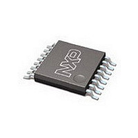
PCA9546PW/G,118 NXP Semiconductors, PCA9546PW/G,118 Datasheet - Page 6

PCA9546PW/G,118
Manufacturer Part Number
PCA9546PW/G,118
Description
Manufacturer
NXP Semiconductors
Datasheet
1.PCA9546PWG118.pdf
(17 pages)
Specifications of PCA9546PW/G,118
Logical Function
I2C Multiplexer
Configuration
1 x 4:1
Number Of Inputs
4
Number Of Outputs
1
Operating Supply Voltage (typ)
2.5/3.3/5V
Operating Supply Voltage (min)
2.3V
Operating Supply Voltage (max)
5.5V
Power Dissipation
400mW
Operating Temp Range
-40C to 85C
Operating Temperature Classification
Industrial
Mounting
Surface Mount
Pin Count
16
Package Type
TSSOP
Lead Free Status / Rohs Status
Compliant
Philips Semiconductors
VOLTAGE TRANSLATION
The pass gate transistors of the PCA9546 are constructed such that
the V
be passed from one I
2004 Sep 30
V
4-channel I
pass
DD
5.0
4.5
4.0
3.5
3.0
2.5
2.0
1.5
1.0
voltage can be used to limit the maximum voltage that will
2.0
2.5
Figure 5. V
2
TYPICAL
2
C-bus to another.
C switch with reset
3.0
pass
V
pass
MAXIMUM
3.5
vs. V
voltage vs. V
DD
V
4.0
DD
4.5
DD
MINIMUM
5.0
SW00820
5.5
6
Figure 5 shows the voltage characteristics of the pass gate
transistors (note that the PCA9546 is only tested at the points
specified in the DC Characteristics section of this datasheet). In
order for the PCA9546 to act as a voltage translator, the V
voltage should be equal to, or lower than the lowest bus voltage. For
example, if the main bus was running at 5 V, and the downstream
buses were 3.3 V and 2.7 V, then V
2.7 V to effectively clamp the downstream bus voltages. Looking at
Figure 5, we see that V
PCA9546 supply voltage is 3.5 V or lower so the PCA9546 supply
voltage could be set to 3.3 V. Pull-up resistors can then be used to
bring the bus voltages to their appropriate levels (see Figure 12).
More Information can be found in Application Note AN262 PCA954X
family of I
2
C/SMBus multiplexers and switches.
pass
(max.) will be at 2.7 V when the
pass
should be equal to or below
PCA9546
Product data sheet
pass


