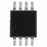
TS4902IST STMicroelectronics, TS4902IST Datasheet

TS4902IST
Specifications of TS4902IST
TS4902IST
Available stocks
Related parts for TS4902IST
TS4902IST Summary of contents
Page 1
... D = Small Outline Package (SO) - also available in Tape & Reel (DT) January 2002 WITH STANDBY MODE ACTIVE LOW PIN CONNECTIONS (top view) TYPICAL APPLICATION SCHEMATIC Audio Input Rin Cin Package VCC ST D Rstb TS4902 TS4902IS-TS4902IST - MiniSO8 TS4902ID-TS4902IDT - SO8 Cfeed Rfeed VCC Vin Vout Vin+ ...
Page 2
TS4902 ABSOLUTE MAXIMUM RATINGS Symbol 1) V Supply voltage Input Voltage i T Operating Free Air Temperature Range oper T Storage Temperature stg T Maximum Junction Temperature j R Thermal Resistance Junction to Ambient thja SO8 MiniSO8 ...
Page 3
ELECTRICAL CHARACTERISTICS V = +5V, GND = 0V 25°C (unless otherwise specified) CC amb Symbol Supply Current input signal, no load 1) Standby Current I STANDBY No input signal, Vstdby = GND ...
Page 4
TS4902 ELECTRICAL CHARACTERISTICS V = 2.6V, GND = 0V 25°C (unless otherwise specified) CC amb Symbol Supply Current input signal, no load 1) Standby Current I STANDBY No input signal, Vstdby = GND ...
Page 5
Fig Open Loop Frequency Response 60 Gain Vcc = Tamb = Phase 20 0 -20 -40 0 100 1000 Frequency (kHz) Fig Open Loop Frequency Response 80 ...
Page 6
TS4902 Fig Open Loop Frequency Response 100 80 Phase 60 Gain Vcc = 560pF -20 Tamb = 25 C -40 0 100 1000 Frequency (kHz) Fig Open Loop ...
Page 7
Fig Power Supply Rejection Ratio (PSRR) vs Power supply -30 Vripple = 200mVrms Rfeed = 22k -40 Input = floating Tamb = 25 C -50 Vcc = 5V to 2.2V - ...
Page 8
TS4902 Fig Pout @ THD + Supply Voltage & 0 1kHz BW < 125kHz 4 Tamb = 25 C 0.6 0.4 ...
Page 9
Fig Output Power vs Load Resistance 1.0 0.8 Vcc=5V 0.6 Vcc=4.5V Vcc=4V 0.4 0.2 Vcc=3.5V Vcc=3V Vcc=2.5V 0 Load Resistance (ohm) Fig Clipping Voltage vs Supply Voltage 1.0 Tamb = 25 C 0.9 ...
Page 10
TS4902 Fig THD + N vs Output Power Vcc = Cin = < 125kHz Tamb = 20kHz 20Hz, 1kHz 0.1 1E-3 0.01 ...
Page 11
Fig THD + N vs Output Power Vcc = Cin = < 125kHz Tamb = 20Hz, 1kHz 20kHz 0.1 1E-3 0.01 0.1 ...
Page 12
TS4902 Fig THD + N vs Output Power Vcc = Cin = < 125kHz 1 Tamb = 25 C 20kHz 0.1 20Hz, 1kHz 0.01 ...
Page 13
Fig Signal to Noise Ratio vs Power Supply with Unweighted Filter (20Hz to 20kHz) 100 90 RL=8 RL= 2.5 3.0 3.5 4.0 Vcc (V) Fig Signal to Noise Ratio vs Power Supply ...
Page 14
TS4902 Fig Current Consumption vs Standby Voltage @ Vcc = 3. 0.0 0.5 1.0 1.5 2.0 Vstandby (V) 14/19 Fig Current Consumption vs Standby Voltage @ Vcc = 2.6V ...
Page 15
BTL Configuration Principle The TS4902 is a monolithic power amplifier with a BTL (Bridge Tied Load) output configuration. BTL means that each end of the load is connected to two single ended output amplifiers. Thus, we have: Single ended output ...
Page 16
TS4902 The efficiency is the ratio between the output power and the power supply ----------------------- - = ---------------------- - Psup ply The maximum theoretical value is reached when Vpeak = Vcc, so ---- - = 78.5% ...
Page 17
At power OFF of the supply discharged by a constant current Icc. The discharge time from 5Cs t = ------------- - = Icc Now, ...
Page 18
TS4902 PACKAGE MECHANICAL DATA 8 PINS - PLASTIC MICROPACKAGE (SO Dim. Min 0 0.65 b 0.35 b1 0. 4 3.8 L 0.4 ...
Page 19
... No license is granted by implication or otherwise under any patent or patent rights of STMicroelectronics. Specifications mentioned in this publication are subject to change without notice. This publication supersedes and replaces all information previously supplied ...


