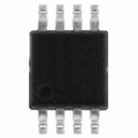
TS4902IST STMicroelectronics, TS4902IST Datasheet - Page 16

TS4902IST
Manufacturer Part Number
TS4902IST
Description
IC AMP AUDIO PWR .7W MONO 8MSOP
Manufacturer
STMicroelectronics
Type
Class ABr
Datasheet
1.TS4902IST.pdf
(19 pages)
Specifications of TS4902IST
Output Type
1-Channel (Mono)
Max Output Power X Channels @ Load
700mW x 1 @ 8 Ohm
Voltage - Supply
2.2 V ~ 5.5 V
Features
Depop, Standby, Thermal Protection
Mounting Type
Surface Mount
Package / Case
8-MSOP, Micro8™, 8-uMAX, 8-uSOP,
Lead Free Status / RoHS Status
Lead free / RoHS Compliant
Other names
497-8116-2
TS4902IST
TS4902IST
Available stocks
Company
Part Number
Manufacturer
Quantity
Price
TS4902
The efficiency is the ratio between the output
power and the power supply
The maximum theoretical value is reached when
Vpeak = Vcc, so
Two capacitors are needed to bypass properly the
TS4902, a power supply bypass capacitor Cs and
a bias voltage bypass capacitor Cb.
Cs has especially an influence on the THD+N in
high frequency (above 7kHz) and indirectly on the
power supply disturbances.
With 100µF, you can expect similar THD+N
performances like shown in the datasheet.
If Cs is lower than 100µF, in high frequency
increases, THD+N and disturbances on the power
supply rail are less filtered.
To the contrary, if Cs is higher than 100µF, those
disturbances on the power supply rail are more
filtered.
Cb has an influence on THD+N in lower frequency,
but its function is critical on the final result of PSRR
with input grounded in lower frequency.
If Cb is lower than 1µF, THD+N increase in lower
frequency (see THD+N vs frequency curves) and
the PSRR worsens up
If Cb is higher than 1µF, the benefit on THD+N in
lower frequency is small but the benefit on PSRR
is substantial (see PSRR vs. Cb curve : fig.12).
Note that Cin has a non-negligible effect on PSRR
in lower frequency. Lower is its value, higher is the
PSRR (see fig. 13).
Pop and Click performance is intimately linked
with the size of the input capacitor Cin and the bias
voltage bypass capacitor Cb.
Size of Cin is due to the lower cut-off frequency
and PSRR value requested. Size of Cb is due to
THD+N and PSRR requested always in lower
frequency.
16/19
Decoupling of the circuit
Pop and Click performance
=
----------------------- - =
Psup ply
P
---- - = 78.5%
4
O UT
---------------------- -
4V
V
P E A K
C C
Moreover, Cb determines the speed that the
amplifier turns ON. The slower the speed is, the
softer the turn ON noise is.
The charge time of Cb is directly proportional to
the internal generator resistance 50k .
Then, the charge time constant for Cb is
As Cb is directly connected to the non-inverting
input (pin 2 & 3) and if we want to minimize, in
amplitude and duration, the output spike on Vout1
(pin 5), Cin must be charged faster than Cb. The
charge time constant of Cin is
Thus we have the relation
The respect of this relation permits to minimize the
pop and click noise.
Remark : Minimize Cin and Cb has a benefit on
pop and click phenomena but also on cost and
size of the application.
Example : your target for the -3dB cut off
frequency is 100 Hz. With Rin=Rfeed=22 k ,
Cin=72nF (in fact 82nF or 100nF).
With Cb=1µF, if you choose the one of the latest
two values of Cin, the pop and click phenomena at
power supply ON or standby function ON/OFF will
be very small
50 k x1µF >> 44k x100nF (50ms >> 4.4ms).
Increasing Cin value increases the pop and click
phenomena to an unpleasant sound at power
supply ON and standby function ON/OFF.
Why Cs is not important in pop and click
consideration ?
Hypothesis :
• Cs = 100µF
• Supply voltage = 5V
• Supply voltage internal resistor = 0.1
• Supply current of the amplifier Icc = 6mA
At power ON of the supply, the supply capacitor is
charged through the internal power supply
resistor. So, to reach 5V you need about five to ten
times the charging time constant of Cs ( s =
0.1xCs (s)).
Then, this time equal 50µs to 100µs << b in the
majority of application.
b = 50k xCb (s)
in = (Rin+Rfeed)xCin (s)
in << b (s)


