LM4781TA/NOPB National Semiconductor, LM4781TA/NOPB Datasheet - Page 16
LM4781TA/NOPB
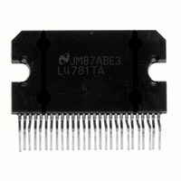
Manufacturer Part Number
LM4781TA/NOPB
Description
IC AMP AUDIO PWR 35W AB TO220-27
Manufacturer
National Semiconductor
Series
Overture™r
Type
Class ABr
Datasheet
1.LM4781TANOPB.pdf
(25 pages)
Specifications of LM4781TA/NOPB
Output Type
3-Channel
Max Output Power X Channels @ Load
35W x 3 @ 8 Ohm
Voltage - Supply
20 V ~ 70 V, ±10 V ~ 35 V
Features
Depop, Mute, Short-Circuit and Thermal Protection
Mounting Type
Through Hole
Package / Case
TO-220-27 (Bent and Staggered Leads)
For Use With
LM4781TABD - BOARD EVALUATION LM4781TA
Lead Free Status / RoHS Status
Lead free / RoHS Compliant
Other names
*LM4781TA
*LM4781TA/NOPB
LM4781TA
*LM4781TA/NOPB
LM4781TA
Available stocks
Company
Part Number
Manufacturer
Quantity
Price
Company:

Part Number:
LM4781TA/NOPB
Manufacturer:
National Semiconductor
Quantity:
135


www.national.com
Application Information
tics section shows the area of device operation where
SPiKe Protection Circuitry is not enabled. The SPiKe Pro-
tection Response waveform graph shows the waveform dis-
tortion when SPiKe is enabled. Please refer to AN-898 for
more detailed information.
THERMAL PROTECTION
The LM4781 has a sophisticated thermal protection scheme
to prevent long-term thermal stress of the device. When the
temperature on the die exceeds 150˚C, the LM4781 shuts
down. It starts operating again when the die temperature
drops to about 145˚C, but if the temperature again begins to
rise, shutdown will occur again above 150˚C. Therefore, the
device is allowed to heat up to a relatively high temperature
if the fault condition is temporary, but a sustained fault will
cause the device to cycle in a Schmitt Trigger fashion be-
tween the thermal shutdown temperature limits of 150˚C and
145˚C. This greatly reduces the stress imposed on the IC by
thermal cycling, which in turn improves its reliability under
sustained fault conditions.
Since the die temperature is directly dependent upon the
heat sink used, the heat sink should be chosen so that
thermal shutdown is not activated during normal operation.
Using the best heat sink possible within the cost and space
constraints of the system will improve the long-term reliability
of any power semiconductor device, as discussed in the
Determining the Correct Heat Sink section.
DETERMlNlNG MAXIMUM POWER DISSIPATION
Power dissipation within the integrated circuit package is a
very important parameter requiring a thorough understand-
ing if optimum power output is to be obtained. An incorrect
maximum power dissipation calculation may result in inad-
equate heat sinking causing thermal shutdown and thus
limiting the output power.
Equation (2) shows the theoretical maximum power dissipa-
tion point for each amplifier in a single-ended configuration
where V
Thus by knowing the total supply voltage and rated output
load, the maximum power dissipation point can be calcu-
lated. The package dissipation is three times the number
which results from Equation (2) since there are three ampli-
fiers in each LM4781. Refer to the graphs of Power Dissipa-
tion versus Output Power in the Typical Performance Char-
acteristics section which show the actual full range of power
dissipation not just the maximum theoretical point that re-
sults from Equation (2).
DETERMINING THE CORRECT HEAT SINK
The choice of a heat sink for a high-power audio amplifier is
made entirely to keep the die temperature at a level such
that the thermal protection circuitry is not activated under
normal circumstances.
The thermal resistance from the die to the outside air, θ
(junction to ambient), is a combination of three thermal re-
sistances, θ
(sink to ambient). The thermal resistance, θ
case), of the LM4781T is 0.9˚C/W. Using Thermalloy Ther-
macote thermal compound, the thermal resistance, θ
(case to sink), is about 0.2˚C/W. Since convection heat flow
(power dissipation) is analogous to current flow, thermal
CC
is the total supply voltage.
JC
(junction to case), θ
P
DMAX
= (V
CC
)
2
CS
/ 2π
(case to sink), and θ
2
R
L
(Continued)
JC
(junction to
(2)
SA
CS
JA
16
resistance is analogous to electrical resistance, and tem-
perature drops are analogous to voltage drops, the power
dissipation out of the LM4781 is equal to the following:
where T
ture and θ
Once the maximum package power dissipation has been
calculated using Equation 2, the maximum thermal resis-
tance, θ
be calculated. This calculation is made using Equation 4
which is derived by solving for θ
Again it must be noted that the value of θ
upon the system designer’s amplifier requirements. If the
ambient temperature that the audio amplifier is to be working
under is higher than 25˚C, then the thermal resistance for the
heat sink, given all other things are equal, will need to be
smaller.
SUPPLY BYPASSING
The LM4781 has excellent power supply rejection and does
not require a regulated supply. However, to improve system
performance as well as eliminate possible oscillations, the
LM4781 should have its supply leads bypassed with low-
inductance capacitors having short leads that are located
close to the package terminals. Inadequate power supply
bypassing will manifest itself by a low frequency oscillation
known as “motorboating” or by high frequency instabilities.
These instabilities can be eliminated through multiple by-
passing utilizing a large tantalum or electrolytic capacitor
(10µF or larger) which is used to absorb low frequency
variations and a small ceramic capacitor (0.1µF) to prevent
any high frequency feedback through the power supply lines.
If adequate bypassing is not provided, the current in the
supply leads which is a rectified component of the load
current may be fed back into internal circuitry. This signal
causes distortion at high frequencies requiring that the sup-
plies be bypassed at the package terminals with an electro-
lytic capacitor of 470µF or more.
BRIDGED AMPLIFIER APPLICATION
The LM4781 has three operational amplifiers internally, al-
lowing for a few different amplifier configurations. One of
these configurations is referred to as “bridged mode” and
involves driving the load differentially through two of the
LM4781’s outputs. This configuration is shown in Figure 2.
Bridged mode operation is different from the classical single-
ended amplifier configuration where one side of its load is
connected to ground.
A bridge amplifier design has a distinct advantage over the
single-ended configuration, as it provides differential drive to
the load, thus doubling output swing for a specified supply
voltage. Theoretically, four times the output power is pos-
θ
SA
SA
JMAX
= [(T
JA
, (heat sink to ambient) in ˚C/W for a heat sink can
= θ
= 150˚C, T
JMAX
P
JC
DMAX
−T
+ θ
AMB
CS
= (T
AMB
+ θ
)−P
JMAX
is the system ambient tempera-
SA
DMAX
.
−T
SA
AMB
(θ
in Equation 3.
JC
) / θ
200673B8
+θ
CS
JA
SA
)] / P
is dependent
DMAX
(3)
(4)
Related parts for LM4781TA/NOPB
Image
Part Number
Description
Manufacturer
Datasheet
Request
R

Part Number:
Description:
Audio Power Amplifier IC
Manufacturer:
National Semiconductor
Datasheet:

Part Number:
Description:
National Semiconductor [8-Bit D/A Converter]
Manufacturer:
National Semiconductor
Datasheet:
Part Number:
Description:
National Semiconductor [Media Coprocessor]
Manufacturer:
National Semiconductor
Datasheet:
Part Number:
Description:
Digitally Controlled Tone and Volume Circuit with Stereo Audio Power Amplifier, Microphone Preamp Stage and National 3D Sound
Manufacturer:
National Semiconductor
Datasheet:
Part Number:
Description:
Digitally Controlled Tone and Volume Circuit with Stereo Audio Power Amplifier, Microphone Preamp Stage and National 3D Sound
Manufacturer:
National Semiconductor
Datasheet:
Part Number:
Description:
AC97 Rev 2 Codec with Sample Rate Conversion and National 3D Sound
Manufacturer:
National Semiconductor
Part Number:
Description:
Manufacturer:
National Semiconductor
Datasheet:
Part Number:
Description:
Manufacturer:
National Semiconductor
Datasheet:
Part Number:
Description:
General Purpose, Low Voltage, Low Power, Rail-to-Rail Output Operational Amplifiers
Manufacturer:
National Semiconductor
Datasheet:
Part Number:
Description:
8-bit 20 MSPS flash A/D converter.
Manufacturer:
National Semiconductor
Datasheet:
Part Number:
Description:
Low Noise Quad Operational Amplifier
Manufacturer:
National Semiconductor
Datasheet:
Part Number:
Description:
Quad Differential Line Receivers
Manufacturer:
National Semiconductor
Datasheet:
Part Number:
Description:
Quad High Speed Trapezoidal? Bus Transceiver
Manufacturer:
National Semiconductor
Datasheet:
Part Number:
Description:
Dual Line Receiver
Manufacturer:
National Semiconductor
Datasheet: