SA58672TK,138 NXP Semiconductors, SA58672TK,138 Datasheet
SA58672TK,138
Specifications of SA58672TK,138
SA58672TK-T
SA58672TK-T


Related parts for SA58672TK,138


SA58672TK,138 Summary of contents
Page 1
SA58672 3.0 W mono class-D audio amplifier Rev. 04 — 8 June 2009 1. General description The SA58672 is a mono, filter-free class-D audio amplifier which is available bump WLCSP (Wafer Level Chip-Size Package) and 10-terminal HVSON ...
Page 2
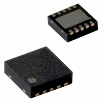
... NXP Semiconductors 3. Applications I Wireless and cellular handsets and PDAs I Portable DVD player I USB speakers I Notebook PC I Portable radio and gaming I Educational toys 4. Ordering information Table 1. Ordering information Type number Package Name Description SA58672TK HVSON10 plastic thermal enhanced very thin small outline package; no leads; ...
Page 3
... NXP Semiconductors 6. Pinning information 6.1 Pinning Fig 2. (1) Exposed Die Attach Paddle (DAP). Fig 4. SA58672_4 Product data sheet SA58672UK bump index area 001aai332 Transparent top view Pin configuration for WLCSP9 terminal 1 index area SD 1 AVDD 2 3 INM 4 INP AGND 5 Transparent top view Pin confi ...
Page 4
... NXP Semiconductors 6.2 Pin description Table 2. Symbol INP AVDD INM AGND PVDD SD OUTM PGND OUTP n.c. DAP 7. Limiting values Table 3. In accordance with the Absolute Maximum Rating System (IEC 60134). Symbol amb stg V ESD SA58672_4 Product data sheet Pin description Pin ...
Page 5
... NXP Semiconductors 8. Static characteristics Table 4. Static characteristics unless otherwise specified amb Symbol Parameter V supply voltage DD V output offset voltage O(offset) PSRR power supply rejection ratio V common-mode input voltage i(cm) CMRR common mode rejection ratio I HIGH-level input current IH I LOW-level input current ...
Page 6
... NXP Semiconductors 9. Dynamic characteristics Table 5. Dynamic characteristics unless otherwise specified amb L Symbol Parameter P output power o THD+N total harmonic distortion-plus-noise output power efficiency po SVRR supply voltage ripple rejection CMRR common mode rejection ratio t delay time from shutdown to d(sd-startup) start-up V output noise voltage ...
Page 7
... NXP Semiconductors 10. Typical characterization curves 100 ( 0.5 1.0 1 4. Fig 5. Output power efficiency as a function of output power 0.5 P (W) 0.4 0.3 0 Fig 6. Power dissipation as a function of output power SA58672_4 Product data sheet 002aad856 (1) 2.0 2.5 3 ...
Page 8
... NXP Semiconductors 400 I DD (mA) 300 (2) (3) 200 100 0 0 0.5 1 8. Fig 7. Supply current as a function of output power (mA 2.5 3.5 (1) With ferrite bead + 1 nF capacitor on outputs 8. (2) Without ferrite beads + 1 nF capacitor on outputs 8. load. L Fig 8. Supply current as a function of supply voltage ...
Page 9
... NXP Semiconductors 2 10 THD+N (%) (1) ( A-weighting THD+N filter Fig 10. Total harmonic distortion-plus-noise as a function of output power SA58672_4 Product data sheet 002aad864 2 10 THD+N (%) ( Rev. 04 — 8 June 2009 SA58672 3.0 W mono class-D audio amplifier 002aad865 (1) (2) (3) ( A-weighting THD+N filter L © NXP B.V. 2009. All rights reserved. ...
Page 10
... NXP Semiconductors 10 THD+N (%) ( dBV 3.5 dBV dBV dBV 2 ( dBV dBV dBV dBV dBV 5 Fig 11. Total harmonic distortion-plus-noise as a function of frequency; R A-weighting THD+N filter SA58672_4 Product data sheet 002aad869 THD+N (%) (2) ( (Hz) 10 THD+N (%) (1) ( (3) ( Rev. 04 — 8 June 2009 3.0 W mono class-D audio amplifier ...
Page 11
... NXP Semiconductors +20 FFT (dB) 40 100 160 kHz kHz i Fig 12. FFT spectrum as a function of frequency; V SA58672_4 Product data sheet 002aad866 +20 FFT (dB) 40 100 160 (kHz +20 FFT (dB) 40 100 160 3 Rev. 04 — 8 June 2009 SA58672 3.0 W mono class-D audio amplifi kHz i 002aad868 ...
Page 12
... NXP Semiconductors 50 SVRR (dB) 70 (3) 90 (1) 110 4.11 ; inputs AC grounded 8.03 ; inputs floating Fig 13. Supply voltage ripple rejection as a function of frequency; G SA58672_4 Product data sheet 002aad873 SVRR (dB) ( (Hz) 50 SVRR (dB) 70 (3) 90 (1) (2) 110 Rev. 04 — 8 June 2009 3.0 W mono class-D audio amplifier ...
Page 13
... NXP Semiconductors 11. Application information 11.1 Power supply decoupling considerations The SA58672 is a mono class-D audio amplifier that requires proper power supply decoupling to ensure the rated performance for THD+N and power efficiency. To decouple high frequency transients, power supply spikes and digital noise on the power bus line, a low Equivalent Series Resistance (ESR) capacitor, of typically placed as close as possible to the PVDD terminals of the device ...
Page 14
... NXP Semiconductors For a required 3 dB cut-off frequency ------------------------------------- - i 2 The input signal may be DC-coupled, but not using input coupling capacitors may increase the output offset voltage. 11.4 PCB layout considerations The component location is very important for performance of the SA58672. Place all external components very close to the device. Placing decoupling capacitors directly at the power supply pins increases effi ...
Page 15
... NXP Semiconductors SV1 GND SD PVDD PVDD GND INM INP GND GND9 GND6 GND R3 and R4 are not populated for differential input drive. For single-ended input drive, either are shorted to ground using a 0 resistor (i.e., one input is AC grounded and the other is driven with the input signal). ...
Page 16
... NXP Semiconductors For applications in which there are circuits that are EMI sensitive to low frequency (< 1 MHz) and there are long leads from amplifier to speaker, it may be necessary to use an LC output filter. 11.7 Efficiency and thermal considerations The maximum ambient operating temperature depends on the heat transferring ability of the heat spreader on the PCB layout ...
Page 17
... NXP Semiconductors 12. Test information 12.1 Test setup for typical characterization curves The SA58672 demo board shown in are used to provide the characterization curves. The test setup diagram in shows the setup details. The output load configuration is comprised of 2 inductors and precision power load resistor. This passive load emulates a small, low power speaker ...
Page 18
... NXP Semiconductors 13. Package outline HVSON10: plastic thermal enhanced very thin small outline package; no leads; 10 terminals; body 0. terminal 1 index area terminal 1 index area DIMENSIONS (mm are the original dimensions) (1) A UNIT max. 0.05 0. 0.2 0.00 0.18 Note 1. Plastic or metal protrusions of 0.075 mm maximum per side are not included. ...
Page 19
... NXP Semiconductors WLCSP9: wafer level chip-size package; 9 bumps; 1.66 x 1.71 x 0.6 mm bump A1 index area bump A1 1 index area DIMENSIONS (mm are the original dimensions) A UNIT max 0.26 0.38 0.34 mm 0.64 0.22 0.34 0.30 OUTLINE VERSION IEC SA58672UK Fig 17. Package outline WLCSP9 SA58672_4 ...
Page 20
... NXP Semiconductors 14. Soldering of SMD packages This text provides a very brief insight into a complex technology. A more in-depth account of soldering ICs can be found in Application Note AN10365 “Surface mount reflow soldering description” . 14.1 Introduction to soldering Soldering is one of the most common methods through which packages are attached to Printed Circuit Boards (PCBs), to form electrical circuits ...
Page 21
... NXP Semiconductors 14.4 Reflow soldering Key characteristics in reflow soldering are: • Lead-free versus SnPb soldering; note that a lead-free reflow process usually leads to higher minimum peak temperatures (see reducing the process window • Solder paste printing issues including smearing, release, and adjusting the process window for a mix of large and small components on one board • ...
Page 22
... NXP Semiconductors Fig 18. Temperature profiles for large and small components For further information on temperature profiles, refer to Application Note AN10365 “Surface mount reflow soldering description” . 15. Soldering of WLCSP packages 15.1 Introduction to soldering WLCSP packages This text provides a very brief insight into a complex technology. A more in-depth account of soldering WLCSP (Wafer Level Chip-Size Packages) can be found in application note AN10439 “ ...
Page 23
... NXP Semiconductors • Solder paste printing issues, such as smearing, release, and adjusting the process window for a mix of large and small components on one board • Reflow temperature profile; this profile includes preheat, reflow (in which the board is heated to the peak temperature), and cooling down imperative that the peak ...
Page 24
... NXP Semiconductors • The bump height on the chip The higher the stand off, the better the stresses are released due to TEC (Thermal Expansion Coefficient) differences between substrate and chip. 15.3.2 Quality of solder joint A flip-chip joint is considered good joint when the entire solder land has been wetted by the solder from the bump ...
Page 25
... NXP Semiconductors Table 9. Acronym LC LSB MP3 MSB PC PCB PDA PSRR PWM RF USB WLCSP 17. Revision history Table 10. Revision history Document ID Release date SA58672_4 20090608 • Modifications: Table 3 “Limiting – Symbol changed from “V – V ESD – V ESD – Added V SA58672_3 20090421 ...
Page 26
... Right to make changes — NXP Semiconductors reserves the right to make changes to information published in this document, including without limitation specifications and product descriptions, at any time and without notice ...
Page 27
... NXP Semiconductors 20. Contents 1 General description . . . . . . . . . . . . . . . . . . . . . . 1 2 Features . . . . . . . . . . . . . . . . . . . . . . . . . . . . . . . 1 3 Applications . . . . . . . . . . . . . . . . . . . . . . . . . . . . 2 4 Ordering information . . . . . . . . . . . . . . . . . . . . . 2 5 Block diagram . . . . . . . . . . . . . . . . . . . . . . . . . . 2 6 Pinning information . . . . . . . . . . . . . . . . . . . . . . 3 6.1 Pinning . . . . . . . . . . . . . . . . . . . . . . . . . . . . . . . 3 6.2 Pin description . . . . . . . . . . . . . . . . . . . . . . . . . 4 7 Limiting values Static characteristics Dynamic characteristics . . . . . . . . . . . . . . . . . . 6 10 Typical characterization curves . . . . . . . . . . . . 7 11 Application information 11.1 Power supply decoupling considerations . . . . 13 11 ...