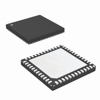
ISL59482IRZ-T13 Intersil, ISL59482IRZ-T13 Datasheet - Page 12

ISL59482IRZ-T13
Manufacturer Part Number
ISL59482IRZ-T13
Description
IC MUX AMP DUAL 500MHZ 48-QFN
Manufacturer
Intersil
Datasheet
1.ISL59482IRZ.pdf
(14 pages)
Specifications of ISL59482IRZ-T13
Applications
4:1 Multiplexer-Amplifier
Number Of Circuits
3
-3db Bandwidth
520MHz
Slew Rate
1600 V/µs
Current - Supply
88mA
Current - Output / Channel
180mA
Mounting Type
Surface Mount
Package / Case
48-VQFN
Lead Free Status / RoHS Status
Lead free / RoHS Compliant
PC Board Layout
The AC performance of this circuit depends greatly on the
care taken in designing the PC board. The following are
recommendations to achieve optimum high frequency
performance from your PC board.
• The use of low inductance components such as chip
• Minimize signal trace lengths. Trace inductance and
• Match channel-channel analog I/O trace lengths and
• Maximize use of AC de-coupled PCB layers. All signal I/O
• Use proper value and location of termination resistors.
• When testing use good quality connectors and cables,
• Minimum of 2 power supply decoupling capacitors are
• The NIC pins are placed on both sides of the input pins.
The QFN Package Requires Additional PCB Layout
Rules for the Thermal Pad
The thermal pad is electrically connected to V- supply
through the high resistance IC substrate. Its primary function
is to provide heat sinking for the IC. However, because of the
connection to the V1- and V2- supply pins through the
substrate, the thermal pad must be tied to the V- supply to
prevent unwanted current flow to the thermal pad. Do not tie
this pin to GND as this could result in large back biased
currents flowing between GND and the V- pins. Maximum
AC performance is achieved if the thermal pad is attached to
a dedicated decoupled layer in a multi-layered PC board. In
cases where a dedicated layer is not possible, AC
performance may be reduced at upper frequencies.
resistors and chip capacitors is strongly recommended.
capacitance can easily limit circuit performance. Avoid
sharp corners, use rounded corners when possible. Vias
in the signal lines add inductance at high frequency and
should be avoided. PCB traces greater than 1" begin to
exhibit transmission line characteristics with signal rise/fall
times of 1ns or less. High frequency performance may be
degraded for traces greater than one inch, unless strip line
are used.
layout symmetry. This will minimize propagation delay
mismatches.
lines should be routed over continuous ground planes (i.e.
no split planes or PCB gaps under these lines). Avoid vias
in the signal I/O lines.
Termination resistors should be as close to the device as
possible.
matching cable types and keeping cable lengths to a
minimum.
recommended (1000pF, 0.01µF) as close to the devices
as possible. Avoid vias between the cap and the device
because vias add unwanted inductance. Larger caps can
be farther away. When vias are required in a layout, they
should be routed as far away from the device as possible.
These pins are not internally connected to the die. It is
recommended these pins be tied to ground to minimize
crosstalk.
12
ISL59482
The thermal pad requirements are proportional to power
dissipation and ambient temperature. A dedicated layer
eliminates the need for individual thermal pad area. When a
dedicated layer is not possible, an isolated thermal pad on
another layer should be used. Pad area requirements should
be evaluated on a case by case basis.
MUX Application Circuits
Each of the two 4:1 triple MUX amplifiers have their own
binary-coded, TTL compatible channel select logic inputs
(S0-1, 2, and S1-1, 2). All three amplifiers are switched
simultaneously from their respective inputs with S0-1 S1-1
controlling MUX-amp1, and S0-2, S1-2 controlling
MUX-amp2.
The HIZ control inputs (HIZ1, HIZ2) and device enable control
inputs (EN1 and EN2) control MUX-amp1 and MUX-amp2 in a
similar fashion. The individual control for each 4:1 triple MUX
enables external connections to configure the device for
different MUX applications.
8:1 RGB Video MUX
For a triple input RGB 8:1 MUX (Figure 4), the RGB amplifier
outputs of MUX-amp1 are parallel-connected to the RGB
amplifier outputs of MUX-amp2 to produce the single RGB
video output. Input channels CH0 to CH3 are assigned to
MUX-amp1, and channels CH4 through CH7 are assigned to
MUX-amp2. Channels CH0 through CH3 are selected by
setting HIZ1 low, HIZ2 high (enables MUX-amp1 and three-
states MUX-amp2) and the appropriate channel select logic
to S0-1, S1-1. Reversing the logic inputs of HIZ1, HIZ2
switches from MUX-amp1 to MUX-amp2 enabling the
selection of channels CH4 through CH7. The channel select
inputs are parallel connected (S0-1 to S0-2) and (S1-1 to
S1-2) to form two logic controls S0, S1. A single S2 control is
split into complimentary logic inputs for HIZ1 and HIZ2 to
produce a chip select function for the MSB. The logic control
truth table is shown in Figure 29.
4:1 RGB Differential Video MUX
Connecting the channel select pins in parallel (S0-1 to S0-2
and S1-1 to S1-2) converts the 8 individual RGB video inputs
into 4 differential RGB input pairs. The amplifier RGB outputs
are similarly paired resulting in a fully differential 4:1 RGB
MUX amp shown in Figure 5. Connecting HIZ1 and HIZ2 to
+5V disables the 4:1 differential MUX, and enables the
connection of additional differential-connected MUX amplifiers
to the same outputs, thus allowing input expansion to 8:1 or
more.
December 22, 2006
FN6209.2


