ISL59483IRZ-T13 Intersil, ISL59483IRZ-T13 Datasheet
ISL59483IRZ-T13
Specifications of ISL59483IRZ-T13


Related parts for ISL59483IRZ-T13

ISL59483IRZ-T13 Summary of contents
Page 1
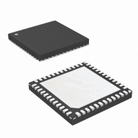
... MARKING REEL ISL59483IRZ ISL59483 IRZ - 48 Ld Exposed Pad 7x7 QFN ISL59483IRZ-T13 ISL59483 IRZ 13” Exposed Pad 7x7 QFN ISL59483EVAL1Z Evaluation PCB NOTE: Intersil Pb-free plus anneal products employ special Pb-free material sets; molding compounds/die attach materials and 100% matte tin plate termination finish, which are RoHS compliant and compatible with both SnPb and Pb-free soldering operations ...
Page 2
Pinout OUTC1 1 OUTB1 2 3 V1- OUTA1 4 V1+ 5 EN1 6 HIZ1 7 IN0C1 8 IN0B1 9 IN0A1 10 GND 11 IN1A1B 12 THERMAL PAD INTERNALLY CONNECTED TO V- PAD MUST BE TIED TO V- Functional Diagram ISL59483 ...
Page 3
... Input Low Current (Logic Inputs ISL59483 Thermal Information = +25°C) Storage Temperature Range . . . . . . . . . . . . . . . . . .-65°C to +150°C Ambient Operating Temperature . . . . . . . . . . . . . . . .-40°C to +85°C Operating Junction Temperature . . . . . . . . . . . . . . .-40°C to +125°C Power Dissipation . . . . . . . . . . . . . . . . . . . . . . . . . . . . . See Curves Pb-free reflow profile . . . . . . . . . . . . . . . . . . . . . . . . . .see link below http://www.intersil.com/pbfree/Pb-FreeReflow.asp = CONDITIONS No load 0V, EN1, EN2 Low IN ...
Page 4
Electrical Specifications V1+ = V2+ = +5V, V1- = V2- = -5V, GND = 0V 5pF unless otherwise specified. (Continued) L PARAMETER DESCRIPTION AC GENERAL PSRR MUX1: Power Supply Rejection Ratio MUX2: Power Supply Rejection Ratio ISO ...
Page 5
Typical Performance Curves 4 SOURCE POWER = -14dBm 2 INTO A 50Ω INPUT IMPEDANCE 4.6pF 12.3pF -10 -12 C INCLUDES 0.3pF -14 L BOARD CAPACITANCE -16 1M 10M FREQUENCY ...
Page 6
Typical Performance Curves OUT P 2.1pF - INCLUDES 0.6pF BOARD CAPACITANCE -10 1M 10M FREQUENCY (Hz) FIGURE 7. MUX2: ...
Page 7
Typical Performance Curves -40 -50 INPUT X TO OUTPUT Y -60 CROSSTALK -70 -80 -90 -100 -110 -120 OFF ISOLATION -130 INPUT X TO OUTPUT X -140 0.1M 1M 10M FREQUENCY (Hz) FIGURE 13. MUX1: CROSSTALK AND OFF ISOLATION 60 ...
Page 8
Typical Performance Curves 0.020 0.016 0.012 0.008 0.004 0.000 -0.004 -0.008 -0.012 -0.016 -0.020 0.02 0.00 -0.02 -0.04 -0.06 -0.08 -0.10 -0.12 -0.14 -0.16 -0.18 -0. (V) OUT FIGURE 19. MUX 2: DIFFERENTIAL ...
Page 9
Typical Performance Curves 2.0 1.0 0.0 TIME (5ns/DIV) FIGURE 24. MUX2 : LARGE SIGNAL TRANSIENT RESPONSE 500Ω INPUT RISE, FALL TIMES V OUT <175ps V = 1.4V OUT P ...
Page 10
Typical Performance Curves S0, S1 50Ω TERM OUT 20ns/DIV FIGURE 30. MUX 1: CHANNEL TO CHANNEL TRANSIENT RESPONSE ENABLE 50Ω TERM OUT 0 20ns/DIV FIGURE ...
Page 11
Typical Performance Curves HIZ 50Ω TERM OUT 10ns/DIV FIGURE 36. MUX 1: HIZ SWITCHING GLITCH V HIZ 50Ω TERM OUT 0 10ns/DIV FIGURE 38. MUX 1: HIZ TRANSIENT RESPONSE ...
Page 12
Pin Description ISL59483 EQUIVALENT (48 LD QFN) PIN NAME CIRCUIT 1 OUTC1 Circuit 3 2 OUTB1 Circuit V1-, V2- Circuit 4A 4 OUTA1 Circuit V1+, V2+ Circuit 4A 6 EN1 Circuit 2 26 EN2 ...
Page 13
Pin Equivalent Circuits CIRCUIT 1 V1+ GNDA1 CAPACITIVELY GNDB1 COUPLED ESD CLAMP GNDC1 V1- CIRCUIT 4A AC Test Circuits ISL59483 50Ω 5pF 75Ω FIGURE 42A. TEST CIRCUIT WITH OPTIMAL OUTPUT LOAD ISL59483 ...
Page 14
V+ SUPPLY LOGIC POWER GND SIGNAL DE-COUPLING CAPS V- SUPPLY If positive voltages are applied to the logic or analog video input pins before V+ is applied, current will flow through the internal ESD diodes to the V+ pin. The ...
Page 15
Use proper value and location of termination resistors. Termination resistors should be as close to the device as possible. • When testing, use good quality connectors and cables, matching cable types and keeping cable lengths to a minimum. • ...
Page 16
... Accordingly, the reader is cautioned to verify that data sheets are current before placing orders. Information furnished by Intersil is believed to be accurate and reliable. However, no responsibility is assumed by Intersil or its subsidiaries for its use; nor for any infringements of patents or other rights of third parties which may result from its use ...
Page 17
Package Outline Drawing L48.7x7B 48 LEAD QUAD FLAT NO-LEAD PLASTIC PACKAGE Rev 0, 12/06 7.00 6 PIN 1 INDEX AREA (4X) 0.15 TOP VIEW ( TYP ) ( 3.70 ) TYPICAL RECOMMENDED LAND PATTERN 17 ISL59483 4X ...