TDF8554J NXP Semiconductors, TDF8554J Datasheet
TDF8554J


Related parts for TDF8554J


TDF8554J Summary of contents
Page 1
... I regulator and two power switches intended for automotive applications. The TDF8554J can operate at a battery voltage as low making this amplifier suitable for stop/start-car operation. The amplifier uses a complementary DMOS output stage in a Silicon-On-Insulator (SOI)-based BCD process. The DMOS output stage ensures a high power output signal with perfect sound quality ...
Page 2
... W power amplifier with multiple voltage regulator safe (with 150 m series impedance and a maximum P 2 C-bus controlled All information provided in this document is subject to legal disclaimers. Rev. 1 — 31 August 2011 TDF8554J = 50 V) and overvoltage P © NXP B.V. 2011. All rights reserved ...
Page 3
... I C-bus IB2[D3:D2 IB2[D3:D2 IB2[D3:D2 0.5 mA I 350 mA TDF8554J/N4 TDF8554J/N2 0.5 mA I 300 mA All information provided in this document is subject to legal disclaimers. Rev. 1 — 31 August 2011 TDF8554J Min Typ 6 14.4 - 260 - 190 ...
Page 4
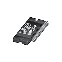
... V V IB1[D7:D4] = 1001 P switch 400 mA O switch 400 mA O Package Name Description DBS37P plastic DIL-bent-SIL power package; 37 leads (lead length 6.8 mm) All information provided in this document is subject to legal disclaimers. Rev. 1 — 31 August 2011 TDF8554J Min Typ 4.75 5.0 5.7 6.0 6.6 7.0 8.1 8.6 5.7 6.0 6.65 7.0 7 ...
Page 5
... GND DIAG CLIP DETECT/ DIAGNOSTIC 9 OUT1+ 7 OUT1- PROTECTION/ DIAGNOSTIC 5 OUT2+ 3 OUT2- PROTECTION/ DIAGNOSTIC 17 OUT3+ 19 OUT3- PROTECTION/ DIAGNOSTIC 21 OUT4+ 23 OUT4- PROTECTION/ DIAGNOSTIC DUMP PROTECTION AMPLIFIER PGND3 aaa-000380 PGND2/TAB PGND4 TDF8554J © NXP B.V. 2011. All rights reserved ...
Page 6
... OUT4+ 21 STB 22 OUT4 PGND4 25 DIAG RST 26 SW2 27 RESCAP 28 29 SW1 30 REG1 REG3 31 GND 32 REG4 33 34 REG5 BUCAP 36 REG2 37 All information provided in this document is subject to legal disclaimers. Rev. 1 — 31 August 2011 TDF8554J aaa-000378 © NXP B.V. 2011. All rights reserved ...
Page 7
... CD player 34 regulator 5 output; supply voltage for display section of radio and CD player All information provided in this document is subject to legal disclaimers. Rev. 1 — 31 August 2011 TDF8554J © NXP B.V. 2011. All rights reserved ...
Page 8
... BUCAP REG2 7. Functional description amplifier section The TDF8554J is a complementary quad Bridge-Tied Load (BTL) audio power amplifier made using SOI-based BCDMOS technology. It contains four independent amplifiers in a BTL configuration. The amplifier remains fully operational at a battery voltage as low Below crank detector is activated to shut down the amplifier without audible plops ...
Page 9
... W power amplifier with multiple voltage regulator 2 C-bus (IB1[D0] = 0), the soft mute is activated and t amp-on t d(fast-mute mode All information provided in this document is subject to legal disclaimers. Rev. 1 — 31 August 2011 TDF8554J ) and as a reference for generating half the be © NXP B.V. 2011. All rights reserved. t off 001aam685 ...
Page 10
... SVR voltage/DC input voltage DC voltage output not filtered to ensure headroom All information provided in this document is subject to legal disclaimers. Rev. 1 — 31 August 2011 TDF8554J mute is activated. During the low V P mute threshold (6 V), and there has been no P mute was set to 5.5 V: discharge of ...
Page 11
... C buffer V P 116 mF NMOS V pulse 80N03L Loss-of-ground tester Test circuit for loss-of-ground test All information provided in this document is subject to legal disclaimers. Rev. 1 — 31 August 2011 TDF8554J 2 C-bus. Pin DIAG is pulled LOW to ) wire of the set (2) (1) 2200 μ DUT in application 001aam695 © ...
Page 12
... P exceeds the maximum value C-bus bus during load dump situations remains All information provided in this document is subject to legal disclaimers. Rev. 1 — 31 August 2011 TDF8554J (1) 2200 μ DUT in application , the device switches off th(ovp) at load dump protection; duration ...
Page 13
... DIAG will remain LOW until amplifier has started yes can be enabled if IB4[D2 yes yes yes no no All information provided in this document is subject to legal disclaimers. Rev. 1 — 31 August 2011 TDF8554J = 160 C. j(AV)(pwarn) Figure 7. If this does not reduce the 001aam696 160 170 180 190 T (° ...
Page 14
... Principle of start-up diagnostics SHORTED NORMAL 0.5 Ω 1.5 Ω 1.5 Ω 3.2 Ω Start-up diagnostics load detection levels All information provided in this document is subject to legal disclaimers. Rev. 1 — 31 August 2011 TDF8554J COMPARATORS DOOR-SLAM PROCESSOR 2 I C-BUS BITS LOAD CONDITION 001aam697 Figure 9. LINE DRIVER 20 Ω ...
Page 15
... IB1[D1] turn on diagnostic enable STB amplifier output short All information provided in this document is subject to legal disclaimers. Rev. 1 — 31 August 2011 TDF8554J t d(sudiag-on) (1) (2) t sudiag amp_on 001aam699 speaker fault applied, the shorted channel will report not © NXP B.V. 2011. All rights reserved. ...
Page 16
... C-bus read. Bits DBx[D5] and DBx[D4] indicate the real All information provided in this document is subject to legal disclaimers. Rev. 1 — 31 August 2011 TDF8554J C-bus data bits are set. Toggling the start-up Meaning normal load line driver mode open load invalid: overvoltage or ...
Page 17
... V = (OUT+ - OUT-) o offset threshold read → set bit All information provided in this document is subject to legal disclaimers. Rev. 1 — 31 August 2011 TDF8554J 2 C-bus read of the output offset is 2 C-bus read is performed and the 2 C-bus read time 1 second: read → no offset, DBx[D2] reset ...
Page 18
... C-bus bits not set detection) All information provided in this document is subject to legal disclaimers. Rev. 1 — 31 August 2011 TDF8554J DB1 to 4 [D4] (AC load bit 001aam701 trip level load detected C-bus bits set (V) oM © ...
Page 19
... Line driver mode and low gain mode The TDF8554J amplifier can be used as a line driver low gain amplifier. In both situations, the gain needs to be set via I independently set for front channels (1 and 3) and rear channels (2 and 4). The main difference between the line driver mode and low gain mode is the DC-output voltage ...
Page 20
... If pin STB is LOW, the total quiescent current is low, and the I When pin STB is switched HIGH, the TDF8554J enters operating mode and performs a POR which results in pin DIAG going LOW. The TDF8554J starts when IB1[D0 Bit D0 also resets the ‘power-on reset occurred’ bit (DB2[D7]) and releases pin DIAG. ...
Page 21
... All information provided in this document is subject to legal disclaimers. Rev. 1 — 31 August 2011 2 C-controlled power switches which are . It requires an external capacitor connected to Equation 1: 0.5 of 178 ms (N2) or 321 ms (N4). TDF8554J 2 C-bus. The this capacitor will P ( k L © NXP B.V. 2011. All rights reserved ...
Page 22
... O(REG2) th(rst) falls below the reset threshold value. O(REG2 present, the supply line will not be charged from P All information provided in this document is subject to legal disclaimers. Rev. 1 — 31 August 2011 TDF8554J V BUCAP t out of regulation delay O(REG2) © NXP B.V. 2011. All rights reserved. ...
Page 23
... All information provided in this document is subject to legal disclaimers. Rev. 1 — 31 August 2011 TDF8554J 15. At load dump, all regulator outputs, except I I O(reg) Olim 001aan206 write to TDF8554J read from TDF8554J C-bus and have Hex D8 © NXP B.V. 2011. All rights reserved ...
Page 24
... SDA changes when SCL is HIGH: START condition start − or stop condition SDA SCL data line stable; data valid All information provided in this document is subject to legal disclaimers. Rev. 1 — 31 August 2011 TDF8554J P STOP condition 001aam703 change of data allowed 001aam704 © NXP B.V. 2011. All rights reserved ...
Page 25
... Fig 18. I C-bus read and write modes 2 9.1 I C-bus instruction bytes 2 I C-bus mode: • If R/W bit = 0, the TDF8554J expects five instruction bytes; IB1, IB2, IB3, IB4, IB5 • After a power-on reset, all instruction bits are set to zero Table 9. Bit ...
Page 26
... D3 regulator 1 (audio) control; see D2 D1 enable or disable soft mute all amplifier channels 0 = soft mute off 1 = soft mute on All information provided in this document is subject to legal disclaimers. Rev. 1 — 31 August 2011 TDF8554J …continued Output ( (off) 1 6.0 0 7 ...
Page 27
... D4 temperature pre-warning level 0 = warning level warning level enable or disable channel 1 (RF enable channel disable channel 1 All information provided in this document is subject to legal disclaimers. Rev. 1 — 31 August 2011 TDF8554J …continued Output ( (off) 1 5.0 0 6 ...
Page 28
... below undervoltage level set by IB4[D6] D0 diagnostic bits on DBx4 and DBx5 0 = simple AC/DC-load diagnostic 1 = advanced DC-load diagnostic All information provided in this document is subject to legal disclaimers. Rev. 1 — 31 August 2011 TDF8554J …continued DC output voltage P DC output voltage © NXP B.V. 2011. All rights reserved. ...
Page 29
... W power amplifier with multiple voltage regulator Instruction byte IB5 bit description Symbol Description diagnostics information in bits DBx[D3 short load diagnostic 1 = speaker fault diagnostic All information provided in this document is subject to legal disclaimers. Rev. 1 — 31 August 2011 TDF8554J © NXP B.V. 2011. All rights reserved ...
Page 30
... NXP Semiconductors 2 9.2 I C-bus data bytes If address byte bit R the TDF8554J sends 4 data bytes to the microprocessor DB1, DB2, DB3 and DB4; see All bits are latched. All data bits reset only after reading all 4 data bytes (clear after read), except D4 and D5. ...
Page 31
... D1 channel 3 V short-circuit detection short-circuit short-circuit to V All information provided in this document is subject to legal disclaimers. Rev. 1 — 31 August 2011 TDF8554J Table 18 Table 19 short-circuit detection Table 18 Table © NXP B.V. 2011. All rights reserved. ...
Page 32
... Conditions operating not operating load dump protection for t and t 2 reverse polarity 10 minutes All information provided in this document is subject to legal disclaimers. Rev. 1 — 31 August 2011 TDF8554J Table 18 Table Min Max 6 18 1 + ...
Page 33
... CDM corner pins non-corner pins . P Thermal characteristics Parameter thermal resistance from junction to case thermal resistance from junction to ambient Virtual junction Amplifier 0.5 K/W All information provided in this document is subject to legal disclaimers. Rev. 1 — 31 August 2011 TDF8554J Min Max 40 +105 - 6 [1] 0 ...
Page 34
... C-bus mode on; operating mode selected 0 V < V < 8.5 V STB time after wake-up via pin STB before 2 first I C-bus transmission is recognized; see Figure 3 All information provided in this document is subject to legal disclaimers. Rev. 1 — 31 August 2011 TDF8554J < unless otherwise specified. P Min 6.6 3.0 7.0 5.4 6 ...
Page 35
... IB3[D6:D5 low gain; IB3[D6:D5 normal load high gain (IB3[D6:D5] = 00) low gain (IB3[D6:D5] = 11) line driver load open load All information provided in this document is subject to legal disclaimers. Rev. 1 — 31 August 2011 TDF8554J < unless otherwise specified. P Min [2] - [2] - [2] 250 ...
Page 36
... kHz 250 k ACGND kHz kHz i All information provided in this document is subject to legal disclaimers. Rev. 1 — 31 August 2011 TDF8554J < unless otherwise specified. P Min = DIAG 1 150 125 - - 500 275 - - 18 ...
Page 37
... STB , minimum HIGH-level = 0. and the minimum HIGH-level supply voltage ripple rejection (SVRR) and common mode rejection ratio (CMRR), a resistor cs All information provided in this document is subject to legal disclaimers. Rev. 1 — 31 August 2011 TDF8554J < unless otherwise specified. P Min [ k ...
Page 38
... All information provided in this document is subject to legal disclaimers. Rev. 1 — 31 August 2011 TDF8554J RECTIFIER OUTPUT PEAK BUFFER DETECTOR + 40 dB GAIN 001aam707 maximum kHz (Hz) © NXP B.V. 2011. All rights reserved. ...
Page 39
... 400 mA O 0.5 V I 400 mA O All information provided in this document is subject to legal disclaimers. Rev. 1 — 31 August 2011 TDF8554J Min Typ 10.0 14.4 4.0 - 6.3 - 18.1 22 [1] - 150 V V O(reg2) O(reg2) 0.2 0.1 ...
Page 40
... TDF8554J/N2 TDF8554J/ 120 Hz (p-p) ripple ripple 200 mA BUCAP O TDF8554J/N2 TDF8554J/ 4. 350 mA BUCAP O TDF8554J/N2 TDF8554J/N4 2 0.5 V 0.5 mA I 300 unless otherwise specified O 0.5 mA I 300 mA V ...
Page 41
... IB1[D7:D4] = 1000 12.5 V V IB1[D7:D4] = 1001 f = 120 Hz (p-p) ripple ripple 0 O(reg 300 400 mA O 5 All information provided in this document is subject to legal disclaimers. Rev. 1 — 31 August 2011 TDF8554J amb Min Typ Max 4.75 5.0 5.25 5.7 6.0 6.3 6.6 7.0 7.4 8.1 8.6 9 [4] - 0.6 1 ...
Page 42
... 100 mA P O(reg2) 500 mA BUCAP = d rst and V P Figure 15. BUCAP V (V) V th(rst) t d(rst) All information provided in this document is subject to legal disclaimers. Rev. 1 — 31 August 2011 TDF8554J Min Typ [6] 100 200 - 0.6 - 0.6 0 0.6 - 0.6 0.5 1 0.4 1 0.6 ...
Page 43
... THD + N (%) 1 −1 10 −2 10 − 14 All information provided in this document is subject to legal disclaimers. Rev. 1 — 31 August 2011 TDF8554J 001aan448 (1) ( (Hz) i 001aan449 (1) ( (Hz) i © NXP B.V. 2011. All rights reserved. ...
Page 44
... kHz i = 100 kHz kHz i All information provided in this document is subject to legal disclaimers. Rev. 1 — 31 August 2011 TDF8554J 001aan450 (W) o 001aan451 (W) o © NXP B.V. 2011. All rights reserved ...
Page 45
... 6.2 10 kHz Chan sep (dB) -20 -40 -60 -80 -100 All information provided in this document is subject to legal disclaimers. Rev. 1 — 31 August 2011 TDF8554J 001aam749 (1) (2) (3) (4) 14.2 18 and 2 L 001aam751 (1) ( (Hz and 2 ...
Page 46
... Product data sheet 4 45 W power amplifier with multiple voltage regulator 0 SVRR (dB) −20 −40 −60 −80 −100 All information provided in this document is subject to legal disclaimers. Rev. 1 — 31 August 2011 TDF8554J 001aam753 (Hz) i © NXP B.V. 2011. All rights reserved ...
Page 47
... ACGND PGND1 PGND2/TAB PGND3 PGND4 2.2 μF (4 × 470 nF) (2) simultaneously and protection activated. 0805 case size capacitors (X7R material, P All information provided in this document is subject to legal disclaimers. Rev. 1 — 31 August 2011 TDF8554J 37 REG2 microcontroller 10 μF 100 nF ( REG1 audio 10 μF ...
Page 48
... Fig 31. PCB top view Fig 32. PCB bottom view TDF8554J Product data sheet 4 45 W power amplifier with multiple voltage regulator All information provided in this document is subject to legal disclaimers. Rev. 1 — 31 August 2011 TDF8554J 019aab579 019aab580 © NXP B.V. 2011. All rights reserved ...
Page 49
... Regulator noise figures [1] Noise figure ( 225 750 120 225 320 All information provided in this document is subject to legal disclaimers. Rev. 1 — 31 August 2011 TDF8554J ACGND TDF8554J 2.2 μF 100 Ω aaa-000379 . Table 27 shows the affect of the F = 100 ...
Page 50
... ESR increases to amb 20 ESR (Ω stable region 0 0.1 1 All information provided in this document is subject to legal disclaimers. Rev. 1 — 31 August 2011 TDF8554J Figure 34. To avoid problems maximum ESR 10 100 C (μF) mgl912 © NXP B.V. 2011. All rights reserved ...
Page 51
... 37.8 15 37.4 15.5 REFERENCES JEDEC JEITA - - - - - - All information provided in this document is subject to legal disclaimers. Rev. 1 — 31 August 2011 TDF8554J non-concave view B: mounting base side ...
Page 52
... For PMFP packages hot bar soldering or manual soldering is suitable. TDF8554J Product data sheet 4 45 W power amplifier with multiple voltage regulator Suitability of through-hole mount IC packages for dipping and wave soldering All information provided in this document is subject to legal disclaimers. Rev. 1 — 31 August 2011 TDF8554J stg(max) Soldering method Dipping Wave - suitable ...
Page 53
... EMC IPAS NDMOS PDMOS POR 19. Revision history Table 30. Revision history Document ID Release date TDF8554J v.1 20110831 TDF8554J Product data sheet 4 45 W power amplifier with multiple voltage regulator Abbreviations Description Bipolar Complementary Double-diffused Metal-Oxide Semiconductor Complementary Metal-Oxide Semiconductor Double-diffused Metal-Oxide Semiconductor Digital Signal Processor ...
Page 54
... All information provided in this document is subject to legal disclaimers. Rev. 1 — 31 August 2011 TDF8554J © NXP B.V. 2011. All rights reserved ...
Page 55
... Notice: All referenced brands, product names, service names and trademarks are the property of their respective owners C-bus — logo is a trademark of NXP B.V. http://www.nxp.com salesaddresses@nxp.com All information provided in this document is subject to legal disclaimers. Rev. 1 — 31 August 2011 TDF8554J © NXP B.V. 2011. All rights reserved ...
Page 56
... Soldering of through-hole mount packages. 52 Introduction to soldering through-hole mount packages . . . . . . . . . . . . . . . . . . . . . . . . . . . . 52 Soldering by dipping or by solder wave . . . . . 52 Manual soldering . . . . . . . . . . . . . . . . . . . . . . 52 Package related soldering information Abbreviations . . . . . . . . . . . . . . . . . . . . . . . . . 53 Revision history . . . . . . . . . . . . . . . . . . . . . . . 53 Legal information . . . . . . . . . . . . . . . . . . . . . . 54 Data sheet status . . . . . . . . . . . . . . . . . . . . . . 54 Definitions . . . . . . . . . . . . . . . . . . . . . . . . . . . 54 Disclaimers . . . . . . . . . . . . . . . . . . . . . . . . . . 54 Trademarks . . . . . . . . . . . . . . . . . . . . . . . . . . 55 Contact information . . . . . . . . . . . . . . . . . . . . 55 Contents Date of release: 31 August 2011 Document identifier: TDF8554J All rights reserved. ...