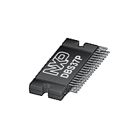
TDF8554J NXP Semiconductors, TDF8554J Datasheet - Page 23

TDF8554J
Manufacturer Part Number
TDF8554J
Description
The TDF8554J is one of a new generation of complementary quad Bridge-Tied Load(BTL) audio power amplifiers with full I²C-bus controlled diagnostics, multiple voltageregulator and two power switches intended for automotive applications
Manufacturer
NXP Semiconductors
Datasheet
1.TDF8554J.pdf
(56 pages)
NXP Semiconductors
9. I
TDF8554J
Product data sheet
2
C-bus specification
8.7 Protection
8.8 Temperature protection
8.9 Switched regulator outputs
All regulator and switch outputs are fully protected against load dump and short-circuit
(foldback current protection); see
the output of regulator 2, will go LOW. The power switches can withstand ‘loss of ground’
which means that pin GND is disconnected and the switch output is connected to ground.
The amplifier is switched off when the regulator junction temperature becomes too high to
prevent undefined audio signals when the regulators are switched off while the amplifier is
still on. A regulator junction temperature that is too high is indicated by pin DIAG and can
be read out via the I
If the junction temperature still increases and the regulator reaches the maximum
temperature protection level, all regulators and switches will be disabled except the
outputs of regulator 2.
Switched outputs (regulator 1, 3, 4 and 5) can be programmed by the I
an internal protection for overtemperature conditions. The regulated outputs, supplying
pulsed current loads, will contaminate the line with high frequency noise, so it is important
to prevent any cross-coupling between the regulated outputs, particularly with the 8.3 V
supply for audio.
Table 8.
A6
1
Fig 15. Foldback current protection
A5
1
TDF8554J hardware address
A4
0
All information provided in this document is subject to legal disclaimers.
V
O(reg)
2
C-bus DB2[D6].
A3
1
Rev. 1 — 31 August 2011
I
A2
1
OS
4 45 W power amplifier with multiple voltage regulator
Figure
A1
0
15. At load dump, all regulator outputs, except
A0
0
R/W
0 = write to TDF8554J;
1 = read from TDF8554J
I
Olim
001aan206
I
O(reg)
TDF8554J
2
© NXP B.V. 2011. All rights reserved.
C-bus and have
Hex
D8
23 of 56


