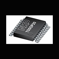
LPC1111FDH20 NXP Semiconductors, LPC1111FDH20 Datasheet - Page 18

LPC1111FDH20
Manufacturer Part Number
LPC1111FDH20
Description
The LPC1111FDH20 is an ARM Cortex-M0 based, low-cost 32-bit MCU, designed for 8/16-bit microcontroller applications, offering performance, low power, simple instruction set and memory addressing together with reduced code size compared to existing 8/
Manufacturer
NXP Semiconductors
Datasheet
1.LPC1110FD20.pdf
(103 pages)
Available stocks
Company
Part Number
Manufacturer
Quantity
Price
NXP Semiconductors
[2]
[3]
[4]
[5]
[6]
Table 7.
LPC111X
Product data sheet
Symbol
PIO0_0 to PIO0_11
RESET/PIO0_0
PIO0_1/CLKOUT/
CT32B0_MAT2
PIO0_2/SSEL0/
CT16B0_CAP0
PIO0_3
PIO0_8/MISO0/
CT16B0_MAT0
PIO0_9/MOSI0/
CT16B0_MAT1
SWCLK/PIO0_10/
SCK0/
CT16B0_MAT2
See
reset the chip and wake up from Deep power-down mode. An external pull-up resistor is required on this pin for the Deep power-down
mode.
5 V tolerant pad providing digital I/O functions with configurable pull-up/pull-down resistors and configurable hysteresis (see
I
5 V tolerant pad providing digital I/O functions with configurable pull-up/pull-down resistors, configurable hysteresis, and analog input.
When configured as a ADC input, digital section of the pad is disabled and the pin is not 5 V tolerant (see
When the system oscillator is not used, connect XTALIN and XTALOUT as follows: XTALIN can be left floating or can be grounded
(grounding is preferred to reduce susceptibility to noise). XTALOUT should be left floating.
2
C-bus pads compliant with the I
Figure 46
LPC1100L series: LPC1112 pin description table (TSSOP20 with V
for the reset pad configuration. RESET functionality is not available in Deep power-down mode. Use the WAKEUP pin to
17
18
19
20
1
2
3
[2]
[3]
[3]
[3]
[3]
[3]
[3]
2
Start
logic
input
yes
yes
yes
yes
yes
yes
yes
C-bus specification for I
All information provided in this document is subject to legal disclaimers.
Type
I/O
I
I/O
I/O
O
O
I/O
I/O
I
I/O
I/O
I/O
O
I/O
I/O
O
I
I/O
I/O
O
Rev. 7 — 1 March 2012
Reset
state
[1]
I; PU
-
I; PU
-
-
I; PU
-
-
I; PU
I; PU
-
-
I; PU
-
-
I; PU
-
-
-
2
C standard mode and I
Description
Port 0 — Port 0 is a 12-bit I/O port with individual direction
and function controls for each bit. The operation of port 0 pins
depends on the function selected through the IOCONFIG
register block.
RESET — External reset input with 20 ns glitch filter. A
LOW-going pulse as short as 50 ns on this pin resets the
device, causing I/O ports and peripherals to take on their
default states, and processor execution to begin at address 0.
PIO0_0 — General purpose digital input/output pin with 10 ns
glitch filter.
PIO0_1 — General purpose digital input/output pin. A LOW
level on this pin during reset starts the ISP command handler.
CLKOUT — Clockout pin.
CT32B0_MAT2 — Match output 2 for 32-bit timer 0.
PIO0_2 — General purpose digital input/output pin.
SSEL0 — Slave Select for SPI0.
CT16B0_CAP0 — Capture input 0 for 16-bit timer 0.
PIO0_3 — General purpose digital input/output pin.
PIO0_8 — General purpose digital input/output pin.
MISO0 — Master In Slave Out for SPI0.
CT16B0_MAT0 — Match output 0 for 16-bit timer 0.
PIO0_9 — General purpose digital input/output pin.
MOSI0 — Master Out Slave In for SPI0.
CT16B0_MAT1 — Match output 1 for 16-bit timer 0.
SWCLK — Serial wire clock.
PIO0_10 — General purpose digital input/output pin.
SCK0 — Serial clock for SPI0.
CT16B0_MAT2 — Match output 2 for 16-bit timer 0.
LPC1110/11/12/13/14/15
2
C Fast-mode Plus.
32-bit ARM Cortex-M0 microcontroller
DDA
and V
SSA
pins)
Figure
© NXP B.V. 2012. All rights reserved.
45).
Figure
18 of 103
45).


