P87C554 NXP Semiconductors, P87C554 Datasheet
P87C554
Available stocks


Related parts for P87C554


P87C554 Summary of contents
Page 1
... P87C554 80C51 8-bit microcontroller – 12 clock operation 16K/512 OTP/RAM 8 channel 10-bit A/D, I capture/compare, high I/O Product data Supersedes data of 1998 Aug 14 hilips Semiconductors INTEGRATED CIRCUITS 2 C, PWM, 2002 Mar 25 ...
Page 2
... Product data P87C554 ...
Page 3
... P87C554 can be expanded using standard TTL compatible memories and logic. In addition, the P87C554 has two software selectable modes of power reduction—idle mode and power-down mode. The idle mode freezes the CPU while allowing the RAM, timers, serial ports, and interrupt system to continue functioning ...
Page 4
... Philips Semiconductors 80C51 8-bit microcontroller – 12 clock operation 16K/512 OTP/RAM, 8 channel 10-bit A/D, I capture/compare, high I/O ORDERING INFORMATION OTP/EPROM P87C554SBAA P87C554SFAA PART NUMBER DERIVATION DEVICE NUMBER (P87C554) OPERATING FREQUENCY MAX (S) P87C554 OTP BLOCK DIAGRAM T0 T1 INT0 INT1 XTAL1 T0, T1 TWO 16-BIT XTAL2 ...
Page 5
... CMT1 P5.7/ADC7 RST EW 63 P5.6/ADC6 64 P5.5/ADC5 65 P5.4/ADC4 66 P5.3/ADC3 67 P5.2/ADC2 68 P5.1/ADC1 SU00208 3 Product data P87C554 LOW ORDER ADDRESS AND DATA BUS SS DD CT0I CT1I CT2I CT3I T2 RT2 SCL SDA HIGH ORDER ADDRESS AND DATA BUS RxD/DATA TxD/CLOCK INT0 INT1 ...
Page 6
... P2M2.x Mode Description 0 0 Pseudo–bidirectional (standard c51 configuration; default Push-Pull 1 0 High impedance 1 1 Open drain P3M1.x P3M2.x Mode Description 0 0 Pseudo–bidirectional (standard c51 configuration; default Push–Pull 1 0 High impedance 1 1 Open drain 4 Product data P87C554 ...
Page 7
... To avoid “latch-up” effect at power-on, the voltage on any pin at any time must not be higher or lower than V respectively. 2002 Mar PWM, NAME AND FUNCTION P4M1.x P4M2.x Mode Description 0 0 Pseudo-bidirectional (standard c51 configuration; default Push-Pull 1 0 High impedance 1 1 Open drain ) during EPROM programming Product data P87C554 + 0 – 0 ...
Page 8
... A15 A14 A13 A12 A11 SDA SCL RT2 T2 CT3I AD7 AD6 AD5 AD4 AD3 6 Product data P87C554 RESET LSB VALUE 00H xxxxxxxxB AADR2 AADR1 AADR0 xx000000B LVADC EXTRAM A0 xxxxx110B O – DPS 000000x0B 00H CTP1 CTN0 ...
Page 9
... TF1 TR1 TF0 TR0 IE1 T2IS1 T2IS0 T2ER T2B0 T2P1 T20V CMI2 CMI1 CMI0 CTI3 7 Product data P87C554 RESET LSB VALUE xx000000B xx000000B 00H 00H 00H 00H 00H 00H GFO PD IDL 00x00000B 00H 00H 00H 00H RP42 ...
Page 10
... RST pin, and a different circuit should be used to perform the power-on reset operation. A timer T3 overflow, if enabled, will force a reset condition to the P87C554 by an internal connection, independent of the level of the RST pin. A reset may be performed in software by setting the software reset bit, SRST (AUXR1 ...
Page 11
... POWER OFF FLAG The Power Off Flag (POF) is set by on-chip circuitry when the V level on the P87C554 rises from The POF bit can be set or cleared by software allowing a user to determine if the reset is the result of a power- warm start after powerdown. The V must remain above 3 V for the POF to remain unaffected by the V level ...
Page 12
... OTP/RAM, 8 channel 10-bit A/D, I capture/compare, high I/O Expanded Data RAM Addressing The P87C554 has internal data memory that is mapped into four separate segments: the lower 128 bytes of RAM, upper 128 bytes of RAM, 128 bytes Special Function Register (SFR), and 256 bytes expanded RAM (EXTRAM). ...
Page 13
... JMP @ A + DPTR MEMORY SU00745A The data pointer can be accessed on a byte-by-byte basis by specifying the low or high byte in an instruction which accesses the SFRs. See application note AN458 for more details. 11 Product data P87C554 FFFF EXTERNAL DATA MEMORY 0100 0000 SU00980 ...
Page 14
... The value read from a reserved bit is indeterminate. 2002 Mar PWM, SRST GF2 WUPD Figure 7. AUXR1: DPTR Control Register 12 Product data P87C554 Reset Value = 0000 00x0B — DSP 1 0 SU01081 ...
Page 15
... SM2 REN TB8 RB8 Description Baud Rate** shift register f /6 OSC 8-bit UART variable 9-bit UART f / /16 OSC OSC 9-bit UART variable Figure 8. S0CON: Serial Port Control Register 13 Product data P87C554 Reset Value = 0000 0000B SU01445 ...
Page 16
... Both slaves can be selected at the same time by an address which has bit (for slave 0) and bit (for slave 1). Thus, both could be addressed with 1100 0000. 14 Product data P87C554 D7 D8 ONLY IN STOP MODE 2, 3 ...
Page 17
... The combination of Timer T2 and the capture and compare logic is very powerful in applications involving rotating machinery, automotive injection systems, etc. Timer T2 and the capture and compare logic are shown in Figure 13. 15 Product data P87C554 ...
Page 18
... Timer T2 halted (off clock source = f OSC 1 0 Test mode; do not use clock source = pin T2 Figure 12. T2 Control Register (TM2CON) 16 Product data P87C554 Reset Value = 00H 1 0 ECT1 ECT0 (LSB) SU01083 Reset Value = 00H 1 0 T2MS1 T2MS0 (LSB) /12 SU01084 ...
Page 19
... TM2IR is set at the end of the following cycle. When a match with CM0 occurs, the controller sets bits 0-5 of port 4 if the corresponding bits of the set enable register STE are at logic 1. 17 Product data P87C554 INT CT3I INT CTI2 CTI3 ...
Page 20
... If “1” then P4.2 is reset on a match between CM1 and Timer T2 If “1” then P4.1 is reset on a match between CM1 and Timer T2 If “1” then P4.0 is reset on a match between CM1 and Timer T2 Figure 15. Reset/Toggle Enable Register (RTE) 18 Product data P87C554 Reset Value = 00H 1 0 CTN1 CTP0 (LSB) ...
Page 21
... Timer T2 comparator 0 interrupt priority level Timer T2 capture register 3 interrupt priority level Timer T2 capture register 2 interrupt priority level Timer T2 capture register 1 interrupt priority level Timer T2 capture register 0 interrupt priority level Timer 2 Interrupt Priority Register (IP1) 19 Product data P87C554 1 0 Reset Value = C0H SP41 SP40 (LSB) SU01087 ...
Page 22
... OSC OSC If the 8-bit timer overflows, a short internal reset pulse is generated which will reset the P87C554. A short output reset pulse is also generated at the RST pin. This short output pulse (3 machine cycles) may be destroyed if the RST pin is connected to a capacitor. This would not, however, affect the internal reset operation. ...
Page 23
... WLE should be set at different parts of the main program. Serial I/O The P87C554 is equipped with two independent serial ports: SIO0 and SIO1. SIO0 is a full duplex UART port and is similar to the Enhanced UART serial port. SIO1 accommodates the I SIO0: SIO0 is a full duplex serial I/O port identical to that of the Enhanced UART except Time 2 cannot be used as a baud rate generator ...
Page 24
... ADCON.3 as above or by applying a rising edge to external pin STADC. When a conversion is started by applying a rising edge, a low level must be applied to STADC for at least one machine cycle followed by a high level for at least one machine cycle. 22 Product data P87C554 OUTPUT PWM0 BUFFER OUTPUT PWM1 ...
Page 25
... ADC start. The result of a completed conversion remains unaffected provided ADCI = logic 1; a new ADC conversion already in progress is aborted when the idle or power-down mode is entered. The result of a completed conversion (ADCI = logic 1) remains unaffected when entering the idle mode. 23 Product data P87C554 STOP 6 SU00958 ...
Page 26
... OTP/RAM, 8 channel 10-bit A/D, I capture/compare, high I/O 2002 Mar PWM, Start of Conversion SOC RESET SAR [BIT POINTER] = MSB [BIT CONVERSION TIME 1 0 TEST COMPLETE [BIT [BIT POINTER END TEST BIT POINTER END EOC END OF CONVERSION Figure 22. A/D Conversion Flowchart 24 Product data P87C554 SU00959 ...
Page 27
... Conversion completed; start of a new conversion requires ADCI=0 AADR1 AADR0 Selected Analog Channel 0 0 ADC0 (P5. ADC1 (P5. ADC2 (P5. ADC3 (P5. ADC4 (P5. ADC5 (P5. ADC6 (P5. ADC7 (P5.7) Figure 23. ADC Control Register (ADCON) 25 Product data P87C554 0 Reset Value = xx00 0000B AADR0 (LSB) SU00960 ...
Page 28
... C, PWM, Power Reduction Modes and The P87C554 has two reduced power modes of operation: the idle DD mode and the power-down mode. These modes are entered by setting bits in the PCON special function register. When the P87C554 enters the idle mode, the following functions are disabled: ...
Page 29
... MULTIPLEXER C S Figure 25. A/D Input: Equivalent Circuit 101 100 011 010 001 000 QUANTIZATION ERROR q = LSB = q/2 – q/2 SYMMETRICAL QUANTIZATION ERROR Figure 26. Effective Conversion Characteristic 27 Product data P87C554 TO COMPARATOR charged SU00962 SU00963 ...
Page 30
... The five interrupt sources common to the 80C51 are the external interrupts (INT0 and INT1), the timer 0 and timer 1 interrupts (IT0 and IT1), and the serial I/O interrupt (RI or TI). In the P87C554, the standard serial interrupt is called SIO0. The eight Timer T2 interrupts are generated by flags CTI0-CT13, CMI0-CMI2, and by the logical OR of flags T2OV and T2BO ...
Page 31
... C) interrupt priority level high SIO0 (UART) interrupt priority level high Timer 1 interrupt priority level high External interrupt 1 priority level high Timer 0 interrupt priority level high External interrupt 0 priority level high Figure 30. Interrupt Priority Register High (IP0H) 29 Product data P87C554 1 0 ECT1 ECT0 (LSB) SU00755 1 0 ...
Page 32
... External interrupt 1 Timer 1 overflow SIO0 (UART) 2 SIO1 ( capture 0 T2 capture 1 T2 capture 2 T2 capture 3 ADC completion T2 compare 0 T2 compare 1 T2 compare 2 (lowest) T2 overflow 30 Product data P87C554 1 0 PCT1 PCT0 (LSB) SU00764 1 0 PCT0H (LSB) SU00984 NAME VECTOR ADDRESS X0 0003H T0 000BH ...
Page 33
... The I C bus may be used for test and diagnostic purposes The output latches of P1.6 and P1.7 must be set to logic 1 in order to enable SIO1. 2 The P87C554 on-chip I C logic provides a serial interface that 2 meets the I C bus specification and supports all transfer modes (other than the low-speed mode) from and to the I logic handles bytes transfer autonomously ...
Page 34
... S1DAT always contains the last byte present on the bus. Thus, in the event of lost arbitration, the transition from master transmitter to slave receiver is made with the correct data in S1DAT. 32 Product data P87C554 SDA SCL INTERFACE ...
Page 35
... S1DAT SHIFT REGISTER ARBITRATION & SYNC LOGIC TIMING & CONTROL LOGIC SERIAL CLOCK GENERATOR TIMER 1 OVERFLOW S1CON CONTROL REGISTER STATUS BITS STATUS DECODER S1STA STATUS REGISTER 2 C Bus Serial Interface Block Diagram 33 Product data P87C554 8 ACK OSC INTERRUPT 8 8 su00966 ...
Page 36
... The serial interrupt flag (SI) is set, and the stretching continues until the serial interrupt flag is cleared. (1) ( Figure 36. Arbitration Procedure (1) (3) (2) SPACE DURATION Figure 37. Serial Clock Synchronization 34 Product data P87C554 ( ACK SU00967 (1) SU00968 ...
Page 37
... ENS1 should not be used to temporarily release SIO1 from the I2C bus since, when ENS1 is reset, the I2C bus status is lost. The AA flag should be used instead (see description of the AA flag in the following text). 35 Product data P87C554 ...
Page 38
... In this case, no STOP condition is transmitted to the bus. However, the SIO1 hardware behaves STOP condition has been received and switches to the defined “not addressed” slave receiver mode. The STO flag is automatically cleared by hardware. 36 Product data P87C554 ACK SU00969 D0 A SHIFT IN (2) (2) A ...
Page 39
... C-bus specification and cannot be used bus rate of 100kHz cannot be realized due to the fixed divider rates. 37 Product data P87C554 2 C bus while the THE LOCK ATE ITS 2 f DIVIDED BY ...
Page 40
... While AA is reset, SIO1 does not respond to its own slave address or a general call address. However, the I and address recognition may be resumed at any time by setting AA. This means that the AA bit may be used to temporarily isolate SIO1 2 from the I C bus. 38 Product data P87C554 ...
Page 41
... CONTINUES 38H OTHER MST A CONTINUES 68H 78H 80H 39 Product data P87C554 Ç Ç Ç Ç Ç Ç 28H Ç Ç Ç Ç Ç Ç Ç Ç Ç Ç Ç Ç Ç Ç S SLA W Ç Ç Ç Ç Ç Ç Ç ...
Page 42
... TO CORRESPONDING 68H 78H 80H STATES IN SLAVE MODE 2 C BUS. SEE TABLE 7. 40 Product data P87C554 Ç Ç Ç Ç Ç Ç Ç Ç Ç Ç Ç Ç 58H Ç Ç Ç Ç Ç Ç Ç Ç Ç Ç Ç Ç Ç Ç ...
Page 43
... CALL Ç Ç Ç Ç Ç Ç Ç Ç Ç Ç Ç Ç 70H A 78H 2 C BUS. SEE TABLE 8. 41 Product data P87C554 Ç Ç Ç Ç Ç Ç A DATA SLA Ç Ç Ç Ç Ç Ç 80H 80H A0H Ç ...
Page 44
... B0H LAST DATA BYTE TRANSMITTED. SWITCHED TO NOT ADDRESSED SLAVE (AA BIT IN S1CON = “0” BUS. SEE TABLE 9. 42 Product data P87C554 Ç Ç Ç Ç Ç Ç Ç Ç Ç Ç Ç Ç Ç Ç Ç Ç Ç Ç ...
Page 45
... STO flag will be reset STOP condition followed by a START condition will be transmitted; STO flag will be reset bus will be released; not addressed slave will be entered START condition will be transmitted when the bus becomes free 43 Product data P87C554 ...
Page 46
... Data byte will be received; ACK bit will be returned Repeated START condition will be transmitted STOP condition will be transmitted; STO flag will be reset STOP condition followed by a START condition will be transmitted; STO flag will be reset 44 Product data P87C554 ...
Page 47
... SLA or General call address. A START condition will be transmitted when the bus becomes free Switched to not addressed SLV mode; Own SLA will be recognized; General call address will be recognized if S1ADR.0 = logic 1. A START condition will be transmitted when the bus becomes free. 45 Product data P87C554 ...
Page 48
... SLA or General call address. A START condition will be transmitted when the bus becomes free Switched to not addressed SLV mode; Own SLA will be recognized; General call address will be recognized if S1ADR.0 = logic 1. A START condition will be transmitted when the bus becomes free. 46 Product data P87C554 ...
Page 49
... STO flag while the STA flag is still set. No STOP condition is transmitted. The SIO1 hardware behaves STOP condition was received and is able to transmit a START condition. The STO flag is cleared by hardware (see Figure 45). 47 Product data P87C554 RBITRATION bus stays busy indefinitely ...
Page 50
... This status code may be used to vector to a service routine which either attempts the aborted serial transfer again or simply recovers from the error condition as shown in Table 10. 48 Product data P87C554 P S SLA 08H RETRY ...
Page 51
... C bus for its own locations to obtain more bytes of code. Each state routine is part of the SIO1 interrupt routine and handles one of the 26 states. It ends with a RETI instruction which causes a return to the main program. 49 Product data P87C554 (3) SU00977 OUTINE Save PSW Push status code ...
Page 52
... NUMBER OF BYTES AS MASTER SLA+R TRANSMITTED TO SLA HIGHER ADDRESS BYTE INTERRUPT ROUTINE SLAVE TRANSMITTER DATA RAM SLAVE RECEIVER DATA RAM MASTER RECEIVER DATA RAM MASTER TRANSMITTER DATA RAM R1 R0 Figure 47. SIO1 Data Memory Map 50 Product data P87C554 CR0 ...
Page 53
... SIO1 behaves essentially as a passive device. In the master modes, an internal timer may be used to cause a time-out if a serial transfer is not complete after a defined period of time. This time period is 2 defined by the system connected to the I C bus. 2002 Mar PWM, ODES C bus and branches 51 Product data P87C554 ...
Page 54
... Number of bytes to transmit ! or receive as MST. –0x51 ! Contains SLA+R transmitted. –0x50 ! High Address byte for STATE 0 ! till STATE 25. 52 Product data P87C554 ! Generates STOP ! (CR0 = 100kHz) ! Releases BUS and ! ACK ! Releases BUS and ! NOT ACK ! Releases BUS and ! set STA ...
Page 55
... Bus error. st0 0x100 mov S1CON,#ENS1_NOTSTA_STO_NOTSI_AA_CR0 ! clr SI pop psw reti 53 Product data P87C554 ! RESET ! Load own SLA + enable ! general call recognition ! P1.6 High level. ! P1.7 High level. ! Enable SI01 interrupt ! SI01 interrupt low priority ! Initialize SLV funct. ! Transmit 4 bytes. ! SLA+W, Transmit funct. ...
Page 56
... BACKUP,NUMBYTMST pop psw reti : 18, Previous state was STATE 8 or STATE 10, SLA+W have been transmitted, ACK has been received. mts18 0x118 mov psw,#SELRB3 mov S1DAT,@r1 ajmp CON 54 Product data P87C554 ! Load SLA+R/W ! clr SI ! Load SLA+R/W ! clr SI ! Save initial value ...
Page 57
... Arbitration lost in SLA+W or DATA. A new START condition is transmitted when the IIC bus is free again. mts38 0x138 mov S1CON,#ENS1_STA_NOTSTO_NOTSI_AA_CR0 mov NUMBYTMST,BACKUP ajmp RETmt 55 Product data P87C554 ! set STO, clr SI ! JMP if NOT last DATA ! clr SI, set AA ! clr SI, set AA ! set STO, clr SI ...
Page 58
... RETmr mov S1CON,#ENS1_NOTSTA_NOTSTO_NOTSI_AA_CR0 inc r0 pop psw reti : 58, DATA have been received, NOT ACK returned. mrs58 0x158 mov psw,#SELRB3 mov @R0,S1DAT sjmp STOP 56 Product data P87C554 ! clr STA, STO, SI set AA ! set STO, clr SI ! Read received DATA ! clr SI,AA ! clr SI, set AA ...
Page 59
... Arbitration lost in SLA+R/W as MST. General call has been received, ACK returned. STA is set to restart MST mode after the bus is free again. srs78 0x178 mov S1CON,#ENS1_STA_NOTSTO_NOTSI_AA_CR0 mov psw,#SELRB3 ajmp INITSRD 57 Product data P87C554 ! clr SI, set AA ! clr SI, set AA ! Initialize SRD counter ! Initialize SRD counter ...
Page 60
... DATA has been received, NOT ACK has been returned. Recognition of own SLA. General call recognized, if S1ADR. 0–1. srs98 0x198 mov S1CON,#ENS1_NOTSTA_NOTSTO_NOTSI_AA_CR0 pop psw reti 58 Product data P87C554 ! Read received DATA ! clr SI,AA ! clr SI, set AA ! clr SI, set AA ! Read received DATA ! clr SI, set AA ...
Page 61
... B0, Arbitration lost in SLA and R/W as MST. Own SLA+R received, ACK returned. STA is set to restart MST mode after the bus is free again. stsb0 0x1b0 mov S1DAT,STD mov S1CON,#ENS1_STA_NOTSTO_NOTSI_AA_CR0 ajmp INITBASE2 59 Product data P87C554 ! clr SI, set AA ! load DATA in S1DAT ! clr SI, set AA ! load DATA in S1DAT ...
Page 62
... C0, DATA has been transmitted, NOT ACK received. stsc0 0x1c0 mov S1CON,#ENS1_NOTSTA_NOTSTO_NOTSI_AA_CR0 pop psw reti : C8, Last DATA has been transmitted (AA=0), ACK received. stsc8 0x1c8 mov S1CON,#ENS1_NOTSTA_NOTSTO_NOTSI_AA_CR0 pop psw reti 60 Product data P87C554 ! clr SI, set AA ! clr SI, set AA ! clr SI, set AA ...
Page 63
... Nonetheless suggested that conventional precautions be taken to avoid applying greater than the rated maxima. 3. Parameters are valid over operating temperature range unless otherwise specified. All voltages are with respect to V noted. DEVICE SPECIFICATIONS TYPE TYPE P87C554 SBxx versions P87C554 SFxx versions 2002 Mar PWM, SUPPLY VOLTAGE (V) ...
Page 64
... –I OH –I OH Test freq = 1 MHz, T amb Port < Product data P87C554 LIMITS MIN MAX MHz MHz 50 < V max DD –0.5 0.2V –0.1 DD –0.5 0.2V –0.3 DD –0.5 0.3V DD 0.2V +0 0.7V V +0.5 ...
Page 65
... C specification input voltage below 1.5 V will be recognized approximately ALE and PSEN to momentarily fall below the 0 – 0.2 V < AV < 0 (87C554) = 4.977 V. ADC is monotonic with no missing codes. REF+ 63 Product data P87C554 LIMITS MIN MAX UNIT AV –0 –0 ...
Page 66
... Center of a step of the actual transfer curve. 2002 Mar PWM, (2) (1) (5) (4) (3) 1 LSB (ideal 1018 1019 1020 1 LSB = Figure 48. ADC Conversion Characteristic 64 Product data P87C554 Offset Gain error error 1021 1022 1023 1024 AV (LSB ) IN ideal – REF+ REF– ...
Page 67
... Product data P87C554 VARIABLE CLOCK MIN MAX UNIT 3.5 16 MHz 2t –40 ns CLCL t –40 ns CLCL t –30 ns CLCL 4t –100 ns CLCL t –30 ns CLCL 3t –45 ns ...
Page 68
... CLCL 14 t CLCL 14 t CLCL 1 s 0.3 s will be filtered out. Maximum capacitance on bus-lines SDA and CLCL < 285ns (16 MHz (24Hz) > f CLCL 66 Product data P87C554 OUTPUT 1 > 4 > 4 > 4 – 3 < 0.3 s > – t CLCL RD 1 > > ...
Page 69
... RHDX DATA IN t AVDV P2.0–P2.7 OR A8–A15 FROM DPH Figure 50. External Data Memory Read Cycle 67 Product data P87C554 = Time for address valid to ALE low. = Time for ALE low to PSEN low. A0–A7 A8–A15 SU00006 A0–A7 FROM PCL INSTR IN A0–A15 FROM PCH ...
Page 70
... Figure 52. External Clock Drive XTAL1 XHQX XHDX VALID VALID VALID Figure 53. Shift Register Mode Timing 68 Product data P87C554 A0–A7 FROM PCL INSTR IN A8–A15 FROM PCH SU00213 SU00009 SET TI VALID VALID VALID VALID SET RI ...
Page 71
... Figure 54. AC Testing Input/Output Float 2.0V 2.0V 0.8V 0.8V Figure 55. AC Testing Input, Float Waveform repeated START condition STOP condition SU;DAT1 HD;DAT 2 Figure 56. Timing SIO1 (I C) Interface 69 Product data P87C554 SU00215 2.4V 0.45V SU00216 START condition t SU;STA 0 0 BUF t SU;STO 0 0 SU;DAT3 t SU ...
Page 72
... EA, RST, Port 0, and EW. : STADC and ref– through resistors of sufficiently high value such that the sink current into these pins DD 70 Product data P87C554 MAXIMUM ACTIVE MODE TYPICAL ACTIVE MODE MAXIMUM IDLE MODE TYPICAL IDLE MODE 16 SU01116 ) OSC SU00218 ...
Page 73
... Figure 61. I Test Condition, Power Down Mode 5 Port 0 and EW. : RST, STADC, XTAL1 and EA. ss ref– through resistors of sufficiently high value such that the sink current into these pins DD 71 Product data P87C554 DD DD SU00219 SU00220 SU00221 3 ...
Page 74
... EA is latched on Reset and all further programming of the EPROM is disabled. When security bits 1 and 2 are programmed, in addition to the above, verify mode is disabled. When all three security bits are programmed, all of the conditions above apply and all external program memory execution is disabled. 72 Product data P87C554 ...
Page 75
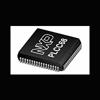
... Philips Semiconductors 80C51 8-bit microcontroller – 12 clock operation 16K/512 OTP/RAM, 8 channel 10-bit A/D, I capture/compare, high I/O PLCC68: plastic leaded chip carrier; 68 leads; pedestal 2002 Mar PWM, 73 Product data P87C554 SOT188-3 ...
Page 76
... OTP/RAM, 8 channel 10-bit A/D, I capture/compare, high I/O REVISION HISTORY Date CPCN 2002 Mar 25 9397 750 09572 1998 Aug 14 9397 750 04273 2002 Mar PWM, Description – PQFP package details removed – References to non-OTP versions removed Previous release 74 Product data P87C554 ...
Page 77
... C, PWM components conveys a license under the Philips’ system provided the system conforms to the Fax: + 24825 Document order number: 75 Product data P87C554 2 C patent Koninklijke Philips Electronics N.V. 2002 All rights reserved. Printed in U.S.A. Date of release: 03-02 9397 750 09572 ...