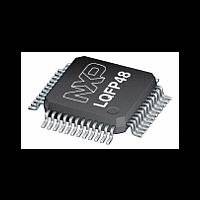
MPT612 NXP Semiconductors, MPT612 Datasheet - Page 7

MPT612
Manufacturer Part Number
MPT612
Description
The MPT612, the first dedicated IC for performing the Maximum Power Point Tracking (MPPT) function, is designed for use in applications that use solar photovoltaic (PV) cells or in fuel cells
Manufacturer
NXP Semiconductors
Datasheet
1.MPT612.pdf
(37 pages)
Available stocks
Company
Part Number
Manufacturer
Quantity
Price
Company:
Part Number:
MPT612FBD48,151
Manufacturer:
ON
Quantity:
22 150
Company:
Part Number:
MPT612FBD48,151
Manufacturer:
NXP Semiconductors
Quantity:
10 000
NXP Semiconductors
MPT612
Product data sheet
Symbol
PVVOLTSENSEBOOST
PVCURRENTSENSE
PIO25/AD6
PIO26/AD7
PIO27/ TRST
PIO28/TMS
PIO29/TCK
PIO30/TDI/MAT3_3
PIO31/TDO
RTCX1
RTCX2
RTCK
XTAL1
XTAL2
JTAGSEL
GND
GNDADC
V
V
RST
DD(ADC)
DDC
Pin
33
34
38
39
8
9
10
15
16
20
25
26
11
12
27
6
7,19,4
3
31
42
5
[1]
[1]
[3]
[3]
[3]
[3]
[1]
[1]
[1]
[8][9]
[8][9]
[8]
Type Description
I
I
I/O
I
I/O
I
I/O
I
I/O
I
I/O
I
I/O
I
O
O
O
I
O
I/O
I
O
I
I
I
I
I
I
All information provided in this document is subject to legal disclaimers.
PV Voltage sense for boost mode; this pin is not connected when only buck
mode is used
PV Current sense.
PIO25: general purpose digital input and output pin.
AD6: analog-to-digital converter input 6
PIO26: general purpose digital input and output pin
AD7: analog-to-digital input 7
PIO27: general purpose digital input and output pin
PIO28: general purpose digital input and output pin.
TMS: Test Mode Select for the JTAG interface
PIO29: General purpose input/output digital pin.
TCK: Test Clock for the JTAG interface
PIO30: general purpose digital input and output pin
TDI: Test Data In for JTAG interface
MAT3_3: PWM output 3 for timer 3
PIO31: general purpose digital output pin
TDO: Test Data Out for JTAG interface
RTC oscillator circuit input; the input voltage must not exceed 1.8 V
RTC oscillator circuit output
Returned test clock output; bidirectional pin with internal pull-up; extra signal
added to the JTAG port. Assists debugger synchronization when processor
frequency varies
oscillator and internal clock generator circuit input; the input voltage must
not exceed 1.8 V
oscillator amplifier output
JTAG interface select; input with internal pull-down:
external reset input; TTL with hysteresis; 5 V tolerant
ground; 0 V reference
analog ground 0 V reference; nominally the same voltage as GND but
should be isolated to minimize noise and error
analog 3.3 V power supply; nominally the same voltage as V
be isolated to minimize noise and error; the level on this pin provides the
ADC voltage reference level
1.8 V core power supply; internal circuitry and on-chip PLL power supply
voltage
TRST : Test Reset for the JTAG interface
Rev. 2 — 14 September 2010
This clock must be slower than
interface to operate
when LOW, the device operates normally
when externally pulled HIGH at reset, PIO27 to PIO31 are configured as
JTAG port and the part is in Debug mode
when LOW, this pin resets the device; all I/O ports and peripherals return
to their default states and processor execution will begin at address 0x00
1
/
6
[6]
Maximum power point tracking IC
of the CPU clock (CCLK) for the JTAG
[6]
[6]
[6]
[6]
© NXP B.V. 2010. All rights reserved.
MPT612
DD(IO)
but should
7 of 7


