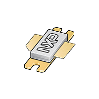
BLF7G20L-200 NXP Semiconductors, BLF7G20L-200 Datasheet - Page 6

BLF7G20L-200
Manufacturer Part Number
BLF7G20L-200
Description
Manufacturer
NXP Semiconductors
Datasheet
1.BLF7G20L-200.pdf
(13 pages)
Available stocks
Company
Part Number
Manufacturer
Quantity
Price
Company:
Part Number:
BLF7G20L-200
Manufacturer:
NXP
Quantity:
5 000
NXP Semiconductors
BLF7G20L-200_7G20LS-200
Product data sheet
Fig 6.
Fig 8.
(dB)
(%)
G
η
(1) f = 1805 MHz
(2) f = 1845 MHz
(3) f = 1880 MHz
D
p
19
18
17
16
15
50
40
30
20
10
0
V
PAR = 8.4 dB at 0.01 % probability on the CCDF.
Power gain and drain efficiency as functions
of average output power; typical values
0
V
PAR = 8.4 dB at 0.01 % probability on the CCDF.
Drain efficiency as a function of average
output power; typical values
DS
DS
= 28 V; I
= 28 V; I
30
30
7.4 2-carrier W-CDMA
η
D
Dq
Dq
= 1620 mA; channel spacing = 5 MHz;
= 1620 mA; channel spacing = 5 MHz;
60
60
90
90
G
p
(1)
(2)
(3)
120
120
All information provided in this document is subject to legal disclaimers.
P
P
014aab194
014aab196
L(AV)
L(AV)
BLF7G20L-200; BLF7G20LS-200
(W)
(W)
150
150
Rev. 4 — 22 July 2011
50
40
30
20
10
(%)
η
D
Fig 7.
Fig 9.
APCR
(dBc)
(dB)
G
(1) f = 1805 MHz
(2) f = 1845 MHz
(3) f = 1880 MHz
(1) f = 1805 MHz
(2) f = 1845 MHz
(3) f = 1880 MHz
19.0
18.5
18.0
17.5
17.0
−10
−20
−30
−40
−50
−60
p
5M
0
0
V
PAR = 8.4 dB at 0.01 % probability on the CCDF.
Power gain as a function of average output
power; typical values
V
PAR = 8.4 dB at 0.01 % probability on the CCDF.
Adjacent power channel ratio (5 MHz) as a
function of average output power;
typical values
DS
DS
= 28 V; I
= 28 V; I
30
30
Dq
Dq
= 1620 mA; channel spacing = 5 MHz;
= 1620 mA; channel spacing = 5 MHz;
(1)
(2)
(3)
60
60
Power LDMOS transistor
90
90
(3)
(2)
(1)
120
120
© NXP B.V. 2011. All rights reserved.
P
P
014aab195
014aab197
L(AV)
L(AV)
(W)
(W)
150
150
6 of 13


