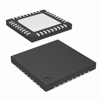
ISL55143IRZ-T Intersil, ISL55143IRZ-T Datasheet

ISL55143IRZ-T
Specifications of ISL55143IRZ-T
Related parts for ISL55143IRZ-T
ISL55143IRZ-T Summary of contents
Page 1
... NUMBER PART (Notes MARKING ISL55141IRZ 55 141IRZ ISL55141IVZ 55141 IVZ ISL55142IRZ 55142 IRZ ISL55142IVZ 55142 IVZ ISL55143IRZ 55143 IRZ NOTES Add “-T*” suffix for tape and reel. Please refer to on reel specifications. V INPX 2. These Intersil Pb-free plastic packaged products employ special ...
Page 2
Pinouts ISL55141 SINGLE DEVICE (16 LD 4X4 QFN) TOP VIEW ISL55142 (20 LD TSSOP) TOP VIEW ...
Page 3
Pin Descriptions PIN V Negative supply input EE Q Channel A, CV reference driven. Comparator output Channel B, CV reference driven. Comparator output Comparator output logic low supply. Unbuffered analog input that sets all ...
Page 4
... Ld TSSOP Package (Notes -0.5V +0.5V QFN Package (Notes 6, 7 TSSOP Package (Notes -0.5V +0.5V TQFN Package (Notes 6, 7 Maximum Junction Temperature (Plastic Plackage Maximum Storage Temperature Range . . . . . . . . . . . -65°C to 150°C Pb-Free Reflow Profile .see link below http://www.intersil.com/pbfree/Pb-FreeReflow.asp SYMBOL MIN ...
Page 5
Electrical Specifications Test Conditions: V otherwise specified. (Continued) PARAMETER Input Capacitance (Note 11) DIGITAL OUTPUTS Output Resistance Output Logic High Voltage Output Logic Low Voltage POWER SUPPLIES, STATIC CONDITIONS Positive Supply DC Current/Comparator Negative Supply ...
Page 6
Test Circuits and Waveforms + 1. 5V INP 1. FIGURE 3. t RECEIVER SWITCHING TEST CIRCUIT PD Application Information The ISL55141, ISL55142, ...
Page 7
The maximum power dissipation allowed in a package is determined according to Equation JMAX AMAX -------------------------------------------- - P = Θ DMAX JA where: • Maximum junction temperature JMAX • Maximum ambient temperature ...
Page 8
... AND 2 CHANNELS ACTIVE CC 100 3200 1600 800 400 200 V SQUARE WAVE PERIOD IN ns INP FIGURE 9. ISL55142 2-CHANNEL ISL55141, ISL55142, ISL55143 Device installed on Intersil ISL55141, ISL55142, ISL55143 Evaluation Boards ISL55143 ISL55142 ISL55141 FIGURE 6. ISL55141 I 200 180 160 140 2 CHANNELS 120 100 80 1 CHANNEL ...
Page 9
... Accordingly, the reader is cautioned to verify that data sheets are current before placing orders. Information furnished by Intersil is believed to be accurate and reliable. However, no responsibility is assumed by Intersil or its subsidiaries for its use; nor for any infringements of patents or other rights of third parties which may result from its use ...
Page 10
... Dimensions D2 and E2 are for the exposed pads which provide improved electrical and thermal performance. 8. Nominal dimensions are provided to assist with PCB Land Pattern Design efforts, see Intersil Technical Brief TB389. 9. Features and dimensions A2, A3, D1, E1, P & θ are present when Anvil singulation method is used and not present for saw singulation ...
Page 11
Package Outline Drawing M14.173 14 LEAD THIN SHRINK SMALL OUTLINE PACKAGE (TSSOP) Rev 3, 10/09 1 5.00 ±0.10 14 6.40 4.40 ±0. 0. 0.65 TOP VIEW H C SEATING PLANE 0.10 C SIDE VIEW ...
Page 12
... Dimensions D2 and E2 are for the exposed pads which provide improved electrical and thermal performance. 8. Nominal dimensions are provided to assist with PCB Land Pattern Design efforts, see Intersil Technical Brief TB389. 9. Features and dimensions A2, A3, D1, E1, P & θ are present when Anvil singulation method is used and not present for saw singulation. 10. Compliant to JEDEC MO-220VHHC Issue I except for the " ...
Page 13
Package Outline Drawing M20.173 20 LEAD THIN SHRINK SMALL OUTLINE PACKAGE (TSSOP) Rev 2, 5/10 1 6.50 ±0.10 20 6.40 4.40 ±0. 0. TOP VIEW H C SEATING PLANE 0.10 C SIDE VIEW (5.65) ...
Page 14
Package Outline Drawing L36.6x6 36 LEAD THIN QUAD FLAT NO-LEAD PLASTIC PACKAGE Rev 5, 08/08 6.00 6 PIN 1 INDEX AREA (4X) 0.15 TOP VIEW ( 5. 4.15) Exp. Dap 4.15) Exp. Dap. ( ...


