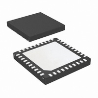
LMH1983SQE/NOPB National Semiconductor, LMH1983SQE/NOPB Datasheet - Page 28

LMH1983SQE/NOPB
Manufacturer Part Number
LMH1983SQE/NOPB
Description
IC VID CLK GEN MULTI RATE 40LLP
Manufacturer
National Semiconductor
Type
Clock Generatorr
Datasheet
1.LMH1983SQENOPB.pdf
(38 pages)
Specifications of LMH1983SQE/NOPB
Applications
Video Equipment
Mounting Type
Surface Mount
Package / Case
40-LLP
Leaded Process Compatible
Yes
Rohs Compliant
Yes
Interface Type
I2C
Supply Voltage (max)
3.3 V
Maximum Operating Temperature
+ 85 C
Minimum Operating Temperature
- 40 C
Mounting Style
SMD/SMT
Peak Reflow Compatible (260 C)
Yes
Lead Free Status / RoHS Status
Lead free / RoHS Compliant
Other names
LMH1983SQETR
Available stocks
Company
Part Number
Manufacturer
Quantity
Price
Part Number:
LMH1983SQE/NOPB
Manufacturer:
TI/德州仪器
Quantity:
20 000
www.national.com
To determine the status of the NOLOCK indication, the
LMH1983 sets up a window where it looks at the amount of
adjustment that is required, over a period of time. Each of
these two parameters is set via a register – the
LOCK_STEP_SIZE register sets the amount of time to look
at the signal over, and the LOCK_THRESHOLD register sets
the amount of variation in the control voltage that can be seen
over this time frame while still considering the device to be
locked.
To minimize the amount of time that it takes to assert lock,
load the LOCK_STEP_SIZE register (register #45, 0x2D )
with a value of 1, and the LOCK_THRESHOLD register (reg-
ister #28, 0x1C) with a value of 31. The effect of this can be
seen in the 'Faster Reaction Mode timing diagram shown be-
low.
VCXO Selection Criteria
The recommended VCXO is CTS part number 357L-
B3C027M0000 which has an absolute pull range of ±50 ppm
and a temperature range of –20°C to +70°C. A VCXO with a
smaller APR can provide better frequency stability, and slight-
ly lower jitter, but the APR must be larger than the anticipated
variation of the input frequency range.
Free-run, Locked and Holdover
Modes
The LMH1983 primary PLL can operate in three different
modes, selected via register 0x05h. In Free-run mode, H
V
by the contents of registers 0x15 and 0x16. By writing to these
registers, the VCXO voltage can be trimmed up or down. the
slave PLLs will remain locked to the primary PLL.
In Genlock mode, the VCXO control voltage is actively con-
trolled to maintain lock between H
frequency. In addition there is a second loop which may take
over to assert a lock between TOF1 and F
on TOF1 alignment for more details.
The third mode is holdover mode. In the event that the refer-
ence is lost, there is an A/D — D/A pair which is able to take
IN
and F
IN
are not used, and the VCXO control voltage is set
IN
and the VCXO output
IN
Faster NOLOCK Reaction Mode timing
. See the section
IN
,
28
over for the PLL control loop, and hold the VCXO control volt-
age constant. For this to work properly, the device has to
realize that it has lost its reference shortly after the reference
is indeed lost. Some sync separators, when the analog input
is lost, will output random pulses from the H, V and F outputs,
which can confuse the device, therefore if holdover mode is
to be used in conjunction with an analog sync separator, it is
best to gate the H, V, F signals with a signal which indicates
if there is a valid reference input.
Control of PLL2 and PLL3
PLL2 and PLL3 have the least amount of flexibility of the four
PLLs in the LMH1983. They are pre-programmed to run at
148.5 MHz and 148.35 MHz respectively. There is a ÷2 option
available to allow the output to be 74.25 MHz or 74.18 MHz
should these frequencies be required. The other controls
available on these two PLLs are to disable them – disabling
PLL2 or PLL3 can save significant amounts of power if that
particular clock is not required.
Control of PLL4
PLL4 is intended to generate a clock for audio use, but has a
lot of versatility built into it. There is access to several registers
which may be used to configure PLL4 to generate any of a
broad selection of frequencies. The default state for PLL4 is
to generate a 24.576 MHz (48 kHz x 512) on the output of
PLL2 / PLL3 Block Diagram
30085165
30085149


