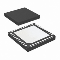
LMH1983SQE/NOPB National Semiconductor, LMH1983SQE/NOPB Datasheet - Page 33

LMH1983SQE/NOPB
Manufacturer Part Number
LMH1983SQE/NOPB
Description
IC VID CLK GEN MULTI RATE 40LLP
Manufacturer
National Semiconductor
Type
Clock Generatorr
Datasheet
1.LMH1983SQENOPB.pdf
(38 pages)
Specifications of LMH1983SQE/NOPB
Applications
Video Equipment
Mounting Type
Surface Mount
Package / Case
40-LLP
Leaded Process Compatible
Yes
Rohs Compliant
Yes
Interface Type
I2C
Supply Voltage (max)
3.3 V
Maximum Operating Temperature
+ 85 C
Minimum Operating Temperature
- 40 C
Mounting Style
SMD/SMT
Peak Reflow Compatible (260 C)
Yes
Lead Free Status / RoHS Status
Lead free / RoHS Compliant
Other names
LMH1983SQETR
Available stocks
Company
Part Number
Manufacturer
Quantity
Price
Part Number:
LMH1983SQE/NOPB
Manufacturer:
TI/德州仪器
Quantity:
20 000
User Defined Formats
There are several registers in the LMH1983 which are loaded
automatically based on the format of the reference that is de-
tected. The LMH1983 allows the user to define a non-stan-
dard format, and the appropriate register values to load into
the registers if that format is detected. In order to identify the
format, the LMH1983 measures the frequency of the Hsync
input, counts the number of lines per frame in the format, and
detects if the particular format is interlaced or progressive.
The Hsync frequency is measured by counting the number of
27 MHz clock edges occur in a period of time equal to 20
Horizontal sync times. To define the frequency the user must
define a minimum permissible count and a maximum count,
thereby setting a window of frequency for Hsync. Registers
0x51 and 0x52 are used to define the 16 bit value for the low
end of the frequency range, while registers 0x53 and 0x54
give the high end of the frequency range. Registers 0x5A and
0x5B are used to define the number of lines per frame for the
format, and bit 4 of register 0x5D is used to indicate if the user
defined format is interlaced or not. Finally bit 7 of 0x5D needs
to be set in order to enable the detection of the user defined
format. Once the user defined format is detected, the contents
of registers 0x55 through 0x59 are used to configure PLL1 to
lock to 27MHz, which is then used as the reference for PLL2,
PLL3 and PLL4.
LMH1983 Typical Interface Circuit
33
Typical Interface Circuit
A typical application circuit for the LMH1983 is shown in the
Typical Interface Circuit. The key areas to consider on this
circuit are the loop filter – which consists of RS, CS, CP and
the LM7711 Operational Amplifier which buffers the loop filter
output prior to driving the control voltage input of the VCXO.
Care must be taken in the component selection for the loop
filter components (see the loop filter discussion above). The
CLKout outputs are differential, LVDS signals, and should be
treated as differential signals. These signals may be laid out
as fully differential lines, in which the characteristic
impedance between the two lines is nominally 100 Ω. Alter-
nately, loosely coupled lines may be used, in which case the
characteristic impedance of each line should be 50 Ω refer-
enced to GND. In either case, care should be taken to match
the lengths of the traces as closely as possible. Trace length
mismatches on a differential line will add to the jitter seen on
that line. Jitter is also added to the clock outputs if other sig-
nals are allowed to interfere with the signal traces, therefore,
to the greatest extent possibly, the clock traces should be
isolated from other signals, especially avoiding long parallel
runs. In places where a hostile signal must cross a sensitive
clock signal, it should be routed such that it crosses as closely
as possible to a 90° crossing.
www.national.com
30085164


