LMH1983SQE/NOPB National Semiconductor, LMH1983SQE/NOPB Datasheet - Page 5
LMH1983SQE/NOPB
Manufacturer Part Number
LMH1983SQE/NOPB
Description
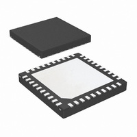
IC VID CLK GEN MULTI RATE 40LLP
Manufacturer
National Semiconductor
Type
Clock Generatorr
Datasheet
1.LMH1983SQENOPB.pdf
(38 pages)
Specifications of LMH1983SQE/NOPB
Applications
Video Equipment
Mounting Type
Surface Mount
Package / Case
40-LLP
Leaded Process Compatible
Yes
Rohs Compliant
Yes
Interface Type
I2C
Supply Voltage (max)
3.3 V
Maximum Operating Temperature
+ 85 C
Minimum Operating Temperature
- 40 C
Mounting Style
SMD/SMT
Peak Reflow Compatible (260 C)
Yes
Lead Free Status / RoHS Status
Lead free / RoHS Compliant
Other names
LMH1983SQETR
Available stocks
Company
Part Number
Manufacturer
Quantity
Price

Part Number:
LMH1983SQE/NOPB
Manufacturer:
TI/德州仪器
Quantity:
20 000


Notes
1. The NO_LOCK status flag is derived from the Lock Status register bits (LOCK1-4) for each PLL. Each lock status bit can be masked from the NO_LOCK flag
by setting their respective mask bits.
2. SDA and SCL pins each require a pull-up resistor of 4.7 kΩ to the VDD supply.
3. XOin must be driven by a 27 MHz clock in order to read or write registers via I
Pin No.
30
31
32
33
34
35
36
37
38
39
40
Pin Name
CLKout1–
CLKout1+
VC_LPF
XOin–
XOin+
Fout2
Fout1
GND
VDD
VDD
VDD
I/O
O
O
O
O
–
–
–
–
I
LVCMOS/LVDS 27 MHz VCXO clock signal for PLL1.
Signal Level
LVCMOS
LVCMOS
Analog
Power
Power
Power
LVDS
GND
5
Video frame timing signal for OUT2 (active low). Timing generator
assignable to PLL1, PLL2, or PLL3. OUT2 format is selectable
via the host.
3.3V supply for CLKout2
3.3V supply for PLL2
– LVCMOS: Directly connect clock signal to XOin+ and bias
XOin- to mid-supply with 0.1uF bypass capacitor.
– LVDS: Directly connect LVDS clock signals to XOin+ and XOin-.
Note: A TCXO or other clean 27 MHz oscillator can be applied
for standalone clock generation using PLLs 2-4 (bypass PLL1).
Video clock from PLL1.
The output is 27 MHz by default and is selectable via the host.
Reference frame timing signal for OUT1 (active Low). Timing
generator fixed to PLL1 OUT1 Format follows the reference input
format.
3.3V supply for CLKout1
Ground
Loop filter for PLL1 charge pump output with VCXO Voltage
Control (VC) sensing.
If free-run and holdover mode, PLL1 is disabled and an internal
DAC outputs a control voltage to the VCXO.
2
C.
Pin Description
www.national.com
Related parts for LMH1983SQE/NOPB
Image
Part Number
Description
Manufacturer
Datasheet
Request
R

Part Number:
Description:
IC VID CLK GEN MULTI RATE 40LLP
Manufacturer:
National Semiconductor
Datasheet:
Part Number:
Description:
National Semiconductor [8-Bit D/A Converter]
Manufacturer:
National Semiconductor
Datasheet:
Part Number:
Description:
National Semiconductor [Media Coprocessor]
Manufacturer:
National Semiconductor
Datasheet:
Part Number:
Description:
Digitally Controlled Tone and Volume Circuit with Stereo Audio Power Amplifier, Microphone Preamp Stage and National 3D Sound
Manufacturer:
National Semiconductor
Datasheet:
Part Number:
Description:
Digitally Controlled Tone and Volume Circuit with Stereo Audio Power Amplifier, Microphone Preamp Stage and National 3D Sound
Manufacturer:
National Semiconductor
Datasheet:
Part Number:
Description:
AC97 Rev 2 Codec with Sample Rate Conversion and National 3D Sound
Manufacturer:
National Semiconductor
Part Number:
Description:
Manufacturer:
National Semiconductor
Datasheet:
Part Number:
Description:
Manufacturer:
National Semiconductor
Datasheet:
Part Number:
Description:
General Purpose, Low Voltage, Low Power, Rail-to-Rail Output Operational Amplifiers
Manufacturer:
National Semiconductor
Datasheet:
Part Number:
Description:
8-bit 20 MSPS flash A/D converter.
Manufacturer:
National Semiconductor
Datasheet:
Part Number:
Description:
Low Noise Quad Operational Amplifier
Manufacturer:
National Semiconductor
Datasheet:
Part Number:
Description:
Quad Differential Line Receivers
Manufacturer:
National Semiconductor
Datasheet:
Part Number:
Description:
Quad High Speed Trapezoidal? Bus Transceiver
Manufacturer:
National Semiconductor
Datasheet:
Part Number:
Description:
Dual Line Receiver
Manufacturer:
National Semiconductor
Datasheet: