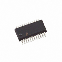
EL4511CUZ-T7 Intersil, EL4511CUZ-T7 Datasheet - Page 20

EL4511CUZ-T7
Manufacturer Part Number
EL4511CUZ-T7
Description
IC VID SYNC SEPARATR HDTV 24QSOP
Manufacturer
Intersil
Type
Synchronous Separatorr
Datasheet
1.EL4511CUZ.pdf
(24 pages)
Specifications of EL4511CUZ-T7
Applications
HDTV, Projectors, Set-Top Boxes
Mounting Type
Surface Mount
Package / Case
24-QSOP
Lead Free Status / RoHS Status
Lead free / RoHS Compliant
Serial Mode Operation
See “Description of Operation” for more details of (Serial
Mode).
Using the Reference Oscillator and Counter
A counter is provided for measuring the vertical time interval;
this counts the clocks at the XTAL pin 1 between vertical
pulses.
This information is not necessary for the operation of the
chip; only for information to the system micro-control. The
count value is read from register 14 at bits 7:6 for the MSBs,
the LSBs are available in register 13, bits 7:0. Register 14,
bit 4 should be a high to indicate that the read operation did
not collide with the up-date timing.
If the crystal oscillator is enabled through the serial interface
(Register 9, bit 6, ENXTAL), the XTAL and XTALN pins will
become the crystal input and crystal output pins for the
32.7kHz crystal. It is also possible to drive the XTAL pin with
a logic level clock up to a maximum of 50kHz; this signal is
only used to measure the vertical rate.
(PIN 24)
XTALN
(PIN 1)
XTAL
20
VERTOUT
FIGURE 10. BLOCK DIAGRAM OF REFERENCE OSCILLATOR
TIMING
REGISTER 9
BIT 6
‘1’
‘0’
EL4511
R
(SEE TABLE 3)
REGISTER 13
LD
CLK
Q0
Q0
DECODE
Example:
Using a 32.768kHz crystal, the count period is 30.52µs. With
a 20ms vertical rate, there will be approximately 656 cycles
(290 Hex) in the "counts per field" registers 13 and 14. With
a 16.666'ms vertical rate, the count of 546 (222 Hex) will be
seen.
Computer & Control Interface
In addition to the mode control pins, the chips default
operating mode may be changed by way of a serial
interface. This is of the three-wire type, Data, clock and
/enable. After the /ENABLE line (pin 5) is taken low, the 16
bits of data on the SDA pin 7 will be clocked into the chip by
the clock signal SCL pin 6. See Figure 10.
The first bit of the data determines whether it will be a read
or write operation. When set to a "0", a write operation will
take place. The following 7 bits, select the register to be
written to. Finally, the last 8 bits are the data to be written or
read. For a read operation, the first bit is a "1".
In general, when registers entries are changed, the
unchanged register bits must have the “Reset Values”
entered as defined by Table 5.
MODE
8
8
10 BIT COUNTER
Q7
Q7
3
Q6
REGISTER 14
Q8
LD
REGISTER 1, BITS 5:3
REGISTER 2, BIT 0
Q7
Q9
TO SERIAL I/F
November 12, 2010
FN7009.8


