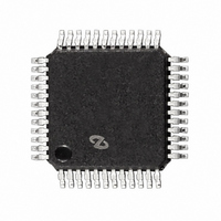
LM98503CCVV National Semiconductor, LM98503CCVV Datasheet - Page 18

LM98503CCVV
Manufacturer Part Number
LM98503CCVV
Description
IC CAMERA SIGNAL PROCESSR 48LQFP
Manufacturer
National Semiconductor
Type
CCD Signal Processor, 10-Bitr
Datasheet
1.LM98503CCVV.pdf
(25 pages)
Specifications of LM98503CCVV
Applications
Video Camera
Mounting Type
Surface Mount
Package / Case
*
Lead Free Status / RoHS Status
Contains lead / RoHS non-compliant
Other names
*LM98503CCVV
Register Data
Register Name Analog Offset 1
Address
Type
Reset Value
Register Name Analog Offset 2
Address
Type
Reset Value
Register Name Analog Offset 3
Address
Type
Reset Value
4.0 Color Filter Array Registers
Register Name Color Filter Array Configuration 0
Address
Type
Reset Value
www.national.com
[7:0]
[7:0]
[7:0]
[7:6]
[5:4]
[3:2]
[1:0]
Bit
Bit
Bit
Bit
Line0:Pixel 1
Signed Analog
Signed Analog
Signed Analog
Line0:Pixel3
Line0:Pixel2
Line0:Pixel0
Gain/Offset
Gain/Offset
Gain/Offset
Gain/Offset
Bit Symbol
Bit Symbol
Bit Symbol
Bit Symbol
Offset
Offset
Offset
5 Hex
Read/Write
0000 0000 Binary
6 Hex
Read/Write
0000 0000 Binary
7 Hex
Read/Write
0000 0000 Binary
8 Hex
Read/Write
0000 0000 Binary
(continued)
2 LSB’s of register addresses
where the gain and offset for pixel
3 of the CFA pattern are stored.
2 LSB’s of register addresses
where the gain and offset for pixel
2 of the CFA pattern are stored.
2 LSB’s of register addresses
where the gain and offset for pixel
1 of the CFA pattern are stored.
2 LSB’s of register addresses
where the gain and offset for pixel
0 of the CFA pattern are stored.
Digital representation of the
analog offset to be applied to
the input of the PGA. See
“Analog Offset” on page 15.
Digital representation of the
analog offset to be applied to
the input of the PGA. See
“Analog Offset” on page 15.
Digital representation of the
analog offset to be applied to
the input of the PGA. See
“Analog Offset” on page 15.
Description
Description
Description
Description
18
Register Name Color Filter Array Configuration 1
Address
Type
Reset Value
Register Name Color Filter Array Definition
Address
Type
Reset Value
5.0 Output Black Level Register
Register Name Output Black Level
Address
Type
Reset Value
6.0 Software Control Registers
Register Name Software Control 0 (Customer)
Address
Type
Reset Value
[7:6]
[5:4]
[3:2]
[1:0]
[3:2]
[2:1]
[7:0]
Bit
Bit
Bit
Bit
[7]
[6]
Line1:Pixel 1
Line 1 Pixels
Line 0 Pixels
Line1:Pixel3
Line1:Pixel2
Line1:Pixel0
Black Level
Gain/Offset
Gain/Offset
Gain/Offset
Gain/Offset
Bit Symbol
Bit Symbol
Bit Symbol
Bit Symbol
Enable
Enable
Output
Output
Offset
Serial
9 Hex
Read/Write
0000 0000 Binary)
A Hex
Read/Write
XXXX 0000 Binary
B Hex
Read/Write
0001 0000 Binary
C Hex
Read/Write
0100 1110 Binary
2 LSB’s of register addresses
where the gain and offset for pixel
3 of the CFA pattern are stored.
2 LSB’s of register addresses
where the gain and offset for pixel
2 of the CFA pattern are stored.
2 LSB’s of register addresses
where the gain and offset for pixel
1 of the CFA pattern are stored.
2 LSB’s of register addresses
where the gain and offset for pixel
0 of the CFA pattern are stored.
Number of pixels in CFA pattern
defined in CFA line 1.
Number of pixels in CFA pattern
defined in CFA line 0.
0 - 256 output black level digital
code value. (see “Output Black
Level” on page 15)
Directs the offset error calculated
by the digital black level correction
loop to the 10 digital output data
pins.
Enables the serial interface output
for reading register values.
Description
Description
Description
Description


