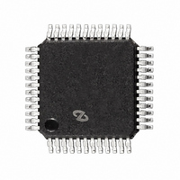
LM98503CCVV National Semiconductor, LM98503CCVV Datasheet - Page 6

LM98503CCVV
Manufacturer Part Number
LM98503CCVV
Description
IC CAMERA SIGNAL PROCESSR 48LQFP
Manufacturer
National Semiconductor
Type
CCD Signal Processor, 10-Bitr
Datasheet
1.LM98503CCVV.pdf
(25 pages)
Specifications of LM98503CCVV
Applications
Video Camera
Mounting Type
Surface Mount
Package / Case
*
Lead Free Status / RoHS Status
Contains lead / RoHS non-compliant
Other names
*LM98503CCVV
Absolute Maximum Ratings
Any Positive Supply Voltage
Voltage On Any Input or Output Pin
Input Current at any pin (Note 3)
Package Input Current (Note 3)
Package Dissipation at T
ESD Susceptibility (Note 5)
Soldering Temperature
Infrared, 10 seconds (Note 6)
Storage Temperature
DC and Logic Level Specifications
The following specifications apply for DV+ = AV+ = DV+ I/O = +3.0V, C
limits apply for TA = T
Power Dissipation Specifications
The following specifications apply for DV+ = AV+ = DV+ I/O = +3.0V, C
limits apply for TA = T
www.national.com
Digital Input Characteristics
Digital Output Characteristics
Power Supply Characteristics
Symbol
Symbol
PWR
VOH
VOL
VIH
IOS
VIL
IIH
IIL
Human Body Model
Machine Model
Output Short Circuit Current
Average Power Dissipation
Logical “1” Output Voltage
Logical “0” Output Voltage
Logical “1” Input Voltage
Logical “0” Input Voltage
Logical “1” Input Current
Logical “0” Input Current
MIN
MIN
A
Parameter
Parameter
= 25°C (Note 4)
to T
to T
MAX
MAX
: all other limits T
: all other limits T
(Notes 1 & 2)
-65°C to 150°C
-0.3V to 4.2V
±35mA
±50mA
DV+ = 3.15V, Iout = -0.5mA
DV+ = 2.85V, Iout = -0.5mA
2500V
260°C
DV+ = 3.15V, Iout = 1.6mA
DV+ = 2.85V, Iout = 1.6mA
VIH = DV+, Reset (internal
A
A
250V
VIH = DV+, Digital inputs
4.2V
AV+ = DV+ = DV+ I/O = 2.7V
AV+ = DV+ = DV+ I/O = 3.0V
= 25
= 25
AV+ = DV+ = DV+ I/O = 3.3
pull-down resistor)
o
except Reset
o
VIL = DGND
Conditions
C (Note 7).
C (Note 7)
Conditions
6
Operating Ratings
Operating Temperature Range
All Supply Voltages
V IN Voltage Range
V
V
V
V
All Digital Inputs Voltage Range
REFT
REFB
REFP
REFN
L
L
= 10pF, and f
= 10pF, and f
Voltage Range
Voltage Range
Voltage Range
Voltage Range
CLK
CLK
(note 9)
Min
2.0
2.5
2.3
= 18MHz unless otherwise noted. Boldface
= 18MHz unless otherwise noted. Boldface
(note 9)
Min
(Notes 1 & 2)
(note 8)
Typical
-100
(note 8)
100
400
Typical
30
100
116
86
+2.85V to +3.15V
-0°C T
-0.05V to 3.35V
(note 9)
(note 9)
Max
Max
2.0V to 2.5V
0.4V to 0.9V
1.3V to 1.9V
1.3V to 1.9V
1.0
0.4
0.4
0.0V to AV+
A
+70°C
Units
mW
Units
mA
nA
nA
V
V
V
V
A


