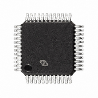
LM98503CCVV National Semiconductor, LM98503CCVV Datasheet - Page 23

LM98503CCVV
Manufacturer Part Number
LM98503CCVV
Description
IC CAMERA SIGNAL PROCESSR 48LQFP
Manufacturer
National Semiconductor
Type
CCD Signal Processor, 10-Bitr
Datasheet
1.LM98503CCVV.pdf
(25 pages)
Specifications of LM98503CCVV
Applications
Video Camera
Mounting Type
Surface Mount
Package / Case
*
Lead Free Status / RoHS Status
Contains lead / RoHS non-compliant
Other names
*LM98503CCVV
Applications Information
3.0 Analog-to-Digital Converter Reference Bypassing
Figure 16 shows a simple reference bypassing scheme with
minimal components. The V
be bypassed to analog ground with 10 F tantalum as well as
0.1 F ceramic capacitors. In a case where the internally
generated reference voltages are not sufficient, the user may
supply external voltages to the reference pins. However, the
reference pin V
Volts. Similarly, V
Volts. Any device used to drive the reference pins should be
able to source adequate current into the V
adequate current from the V
ladder is at its minimum resistivity of 850
The reference voltage at the top of the resistor ladder (V
may be as low as 1.2 Volts above the voltage at the bottom of
the resistor ladder (V
above. V
Volts above ground. However, noise effects will be minimized
and accurate conversions insured when the total reference
voltage is approximately 2.25 Volts and offset from ground by
0.75 Volts.
4.0 Analog Offset DAC Reference Bypassing
The analog offset DAC reference pins, VREFP and VREFN,
should be capacitively bypassed in the same fashion as the
ADC reference pins VREFT and VREFB (See “Analog-to-Digital
Converter Reference Bypassing”).
5.0 Analog Offset DAC Range Adjustment
The analog offset DAC has an input range of 127 LSB (see
“Register Data” on page 17). Each DAC LSB corresponds to
approximately 0.4 LSB at the ADC output. Therefore, the offset
DAC is limited to providing offset values less than or equal to
output may not be sufficient. It is possible to increase the range
of the DAC by adjusting the DAC reference range. The DAC
reference range may be adjusted by lowering the voltage at the
lower DAC reference voltage pin, VREFN, via use of a pull-down
resistor from VREFN to AGND. A resistor value of 1.50k
increase the DAC range by a factor of 2.0x, allowing for offsets
www.national.com
64 LSB at the ADC output. In some applications, this range of
10 F
REFB
Figure 16: Reference Bypassing
may be as low as 0.4 Volts and as high as 0.9
0.1 F
0.1 F
REFT
REFB
AGND
AGND
should be within the range of 2.0 to 2.5
REFB
should be driven in the range of 0.4 to 0.9
) and may be as high as 1.8 Volts
REFB
REFT
AGND
AV+
pin when the reference resistor
and V
V
V
REFB
960
REFT
610
1k
REFB
pins should each
REFT
LM98503
and sink
REFT
will
)
23
of 128 LSB to be applied at the ADC output rather than the
default maximum and minimum offsets of 64 LSB, resulting in a
0.8 LSB DAC step to 1 LSB ADC output step relationship.
Power Supply Considerations
The LM98503 may draw a sufficient amount of current to corrupt
improperly bypassed power supplies. A 10 F to 50 F capacitor
should be placed within 1cm of the analog power (AV+) pins of
the device in parallel with a 0.1 F ceramic chip capacitor placed
as close to the device as layout permits. Leadless chip
capacitors are preferred because they have a low lead
inductance. As is the case with virtually all high-speed
semiconductors, the LM98503 should be assumed to have little
power supply rejection; therefore, a noise-free analog power
source is required.
The analog and digital power supplies of the LM98503 should
be sourced from the same supply voltage, but the supply pins
should be well isolated from one another. Isolating the supplies
prevents digital noise from coupling back into the analog supply
pins. A choke (ferrite bead) is recommended to be placed
between the analog and digital power supply pins as well as a
ceramic chip capacitor placed as close as possible to the analog
supply pin(s) of the device. Additionally, it is not recommended
that the LM98503’s digital supply be used for any other digital
circuitry on the circuit board. All other digital devices should be
powered from a separate digital supply well isolated from both
the analog and digital supplies of the LM98503.
6.0 The LM98503 Clock
Although the LM98503 is tested and its performance guaranteed
with a 18MHz clock, it typically will function with clock
frequencies ranging from 1MHz to 20MHz (see the LM98501 for
conversion speeds greater than 20MHz). Performance is best if
the clock rise and fall times are less than 5ns and the clock trace
is terminated near the clock input pin with a series RC network
consisting of a 100 resistor and a 47pF capacitor.
7.0 Layout and Grounding Techniques
The proper routing of all signals and pertinent grounding
techniques are essential to insure the best signal-to-noise ratio
and dynamic performance possible. Separate analog and digital
ground planes ease meeting the datasheet limits. The analog
ground plane should be low impedance and free from noise of
other components of the system. All bypass capacitors should
be located as close to the pin as possible and connected to the
appropriate ground plane with short traces (<1cm). The analog
input should be isolated from noisy signal traces to avoid
coupling of spurious signals into the input.
Figure 17 provides an example of a suitable layout, including
power supply routing, ground place separation, and bypass
capacitor placement. All input amplifiers, filters, and reference
components should be placed on or over the analog ground
plane. All digital circuitry and I/O lines should be placed over
and grounded via the digital ground plane. Digital and analog
signal lines should never run parallel to each other in close
proximity with each other. These signals should only cross when
absolutely necessary and then only at 90 angles.


