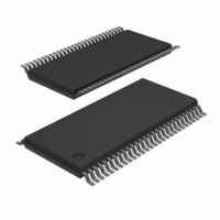
74ALVT16543DGG,118 NXP Semiconductors, 74ALVT16543DGG,118 Datasheet - Page 2

74ALVT16543DGG,118
Manufacturer Part Number
74ALVT16543DGG,118
Description
IC 16BIT REGISTERED TXRX 56TSSOP
Manufacturer
NXP Semiconductors
Series
74ALVTr
Datasheet
1.74ALVT16543DGG112.pdf
(15 pages)
Specifications of 74ALVT16543DGG,118
Logic Type
Registered Transceiver, Non-Inverting
Number Of Elements
2
Number Of Bits Per Element
8
Current - Output High, Low
32mA, 64mA
Voltage - Supply
2.3 V ~ 2.7 V, 3 V ~ 3.6 V
Operating Temperature
-40°C ~ 85°C
Mounting Type
Surface Mount
Package / Case
56-TSSOP
Lead Free Status / RoHS Status
Lead free / RoHS Compliant
Other names
74ALVT16543DG-T
74ALVT16543DG-T
935209940118
74ALVT16543DG-T
935209940118
Philips Semiconductors
FEATURES
QUICK REFERENCE DATA
ORDERING INFORMATION
LOGIC SYMBOL (IEEE/IEC)
2004 Sep 14
56-Pin Plastic SSOP Type III
56-Pin Plastic TSSOP Type II
16-bit universal bus interface
5 V I/O Compatible
3-State buffers
Output capability: +64 mA/–32 mA
TTL input and output switching levels
Input and output interface capability to systems at 5 V supply
Bus-hold data inputs eliminate the need for external pull-up
resistors to hold unused inputs
Live insertion/extraction permitted
Power-up 3-State
Power-up reset
No bus current loading when output is tied to 5 V bus
Latch-up protection exceeds 500mA per JEDEC Std 17
ESD protection exceeds 2000 V per MIL STD 883 Method 3015
and 200 V per Machine Model
2.5 V/3.3 V 16-bit registered transceiver (3-State)
SYMBOL
SYMBOL
I
t
t
C
C
PLH
PHL
CCZ
I/O
IN
PACKAGES
Propagation delay
nAx to nBx or nBx to nAx
Input capacitance DIR, OE
I/O pin capacitance
Total supply current
56
54
55
10
12
13
14
5
6
8
9
PARAMETER
PARAMETER
1
3
2
1EN3 (BA)
G1
1C5
2EN4 (AB)
G2
2C6
6 D
3
TEMPERATURE RANGE
–40 C to +85 C
–40 C to +85 C
5 D
4
C
V
Outputs disabled; V
Outputs disabled
I
L
52
51
49
48
47
45
44
43
= 0 V or V
= 50 pF
2
T
15
16
17
19
20
21
23
24
29
31
30
28
26
27
amb
DESCRIPTION
The 74ALVT16543 is a high-performance BiCMOS product
designed for V
up to 5 V. The device can be used as two 8-bit transceivers or one
16-bit transceiver.
The 74ALVT16543 contains two sets of eight D-type latches, with
separate control pins for each set. Using data flow from A to B as an
example, when the A-to-B Enable (nEAB) input and the A-to-B Latch
Enable (nLEAB) input are LOW, the A-to-B path is transparent.
A subsequent LOW-to-HIGH transition of the nLEAB signal puts the
A data into the latches where it is stored and the B outputs no longer
change with the A inputs. With nEAB and nOEAB both LOW, the
3-State B output buffers are active and display the data present at
the outputs of the A latches.
Control of data flow from B to A is similar, but using the nEBA,
nLEBA, and nOEBA inputs.
Active bus-hold circuitry is provided to hold unused or floating data
inputs at a valid logic level.
CC
= 25 C; GND = 0 V
CONDITIONS
7EN9 (BA)
G7
7C11
8EN10 (AB)
G8
8C12
12 D
I/O
9
= 0 V or V
CC
74ALVT16543DGG
74ALVT16543DL
TYPE NUMBER
operation at 2.5 V or 3.3 V with I/O compatibility
10
11 D
CC
SW00151
42
41
40
38
37
36
34
33
2.5 V
1.8
2.7
40
3
9
TYPICAL
74ALVT16543
3.3 V
1.6
1.8
DWG NUMBER
70
Product data sheet
3
9
SOT371-1
SOT364-1
UNIT
UNIT
pF
pF
ns
A


