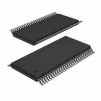
74ALVT16543DGG,118 NXP Semiconductors, 74ALVT16543DGG,118 Datasheet - Page 7

74ALVT16543DGG,118
Manufacturer Part Number
74ALVT16543DGG,118
Description
IC 16BIT REGISTERED TXRX 56TSSOP
Manufacturer
NXP Semiconductors
Series
74ALVTr
Datasheet
1.74ALVT16543DGG112.pdf
(15 pages)
Specifications of 74ALVT16543DGG,118
Logic Type
Registered Transceiver, Non-Inverting
Number Of Elements
2
Number Of Bits Per Element
8
Current - Output High, Low
32mA, 64mA
Voltage - Supply
2.3 V ~ 2.7 V, 3 V ~ 3.6 V
Operating Temperature
-40°C ~ 85°C
Mounting Type
Surface Mount
Package / Case
56-TSSOP
Lead Free Status / RoHS Status
Lead free / RoHS Compliant
Other names
74ALVT16543DG-T
74ALVT16543DG-T
935209940118
74ALVT16543DG-T
935209940118
1. All typical values are at V
2. This is the increase in supply current for each input at the specified voltage level other than V
3. This parameter is valid for any V
4. Unused pins at V
5. I
6. Not guaranteed.
7. For valid test results, data must not be loaded into the flip-flops (or latches) after applying power.
Philips Semiconductors
DC ELECTRICAL CHARACTERISTICS (2.5 V
NOTES:
2004 Sep 14
SYMBOL
2.5 V/3.3 V 16-bit registered transceiver (3-State)
I
a transition time of 100 sec is permitted. This parameter is valid for T
I
I
V
PU/PD
HOLD
HOLD
I
CCZ
V
V
I
I
I
V
V
OFF
I
CCH
CCL
CCZ
RST
EX
I
OH
OH
OL
I
CC
IK
I
is measured with outputs pulled up to V
Input clamp voltage
HIGH-level output voltage
HIGH-level out ut voltage
LOW-level output voltage
Power-up output low voltage
Input leakage current
Off current
Bus Hold current
Data inputs
Current into an output in the
HIGH state when V
Power-up/down 3-State output
current
Quiescent supply current
Additional supply current per
input pin
CC
3
2
PARAMETER
or GND.
6
CC
= 2.5 V and T
O
> V
CC
CC
between 0 V and 1.2 V with a transition time of up to 10 msec. From V
7
amb
V
V
V
V
V
V
V
V
V
V
V
V
V
V
V
V
V
OE/OE = Don’t care
V
I
V
I
V
I
V
Other inputs at V
CC
O
O
O =
CC
CC
CC
CC
CC
CC
CC
CC
CC
CC
CC
CC
CC
CC
CC
O
CC
CC
CC
CC
CC
= 25 C.
= 0 mA
= 0 mA
or pulled down to ground.
= 5.5 V; V
0 mA
= 2.3 V; I
= 2.3 V to 3.6 V; I
= 2.3 V; I
= 2.3 V; I
= 2.3 V; I
= 2.3 V; I
= 2.7 V; I
= 2.7 V; V
= 0 V or 2.7 V; V
= 2.7 V; V
= 2.7 V; V
= 2.7 V; V
= 0 V; V
= 2.3 V; V
= 2.3 V; V
= 2.7 V; Outputs HIGH, V
= 2.7 V; Outputs LOW, V
= 2.7 V; Outputs disabled; V
= 2.3 V to 2.7 V; One input at V
1.2 V; V
5
I
CC
IK
OH
OL
OL
OL
O
or V
0.2 V RANGE)
O
I
I
I
I
I
I
= 1 mA; V
= V
= 5.5 V
= V
= 0 V
= 0.7 V
= 1.7 V
= –18 mA
= 0.5 V to V
TEST CONDITIONS
= 2.3 V
= 100 A
= 24 mA
= 8 mA
CC
= –8 mA
O
CC
CC
= 0 V to 4.5 V
or GND
I
OH
= 5.5 V
or GND
7
= –100 A
amb
I
= V
CC
I
= 25 C only.
I
CC
= GND or V
; V
= GND or V
I
or GND
I
= GND or V
= GND or V
CC
– 0.6 V;
Control pins
Data pins
CC
CC
;
;
CC
CC
CC
;
;
4
4
or GND.
V
Temp = –40 C to +85 C
CC
MIN
1.8
–
–
–
–
–
–
–
–
–
–
–
–
–
–
–
–
–
–
–
CC
– 0.2
= 1.2 V to V
LIMITS
74ALVT16543
–0.85
TYP
0.07
0.04
0.04
0.01
V
120
2.1
0.3
0.1
0.1
0.1
0.1
0.1
0.1
2.6
–6
50
40
CC
–
–
1
CC
Product data sheet
MAX
–1.2
0.55
= 2.5 V
125
100
0.2
0.5
0.4
0.1
4.5
0.1
0.4
10
20
10
–5
100
–
–
–
–
1
UNIT
mA
mA
0.2 V
V
V
V
V
V
A
A
A
A
A
A


