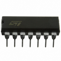
HCF4013BEY STMicroelectronics, HCF4013BEY Datasheet - Page 2

HCF4013BEY
Manufacturer Part Number
HCF4013BEY
Description
IC FLIP FLOP DUAL D-TYPE 14-DIP
Manufacturer
STMicroelectronics
Series
4000Br
Type
D-Typer
Specifications of HCF4013BEY
Function
Set(Preset) and Reset
Output Type
Differential
Number Of Elements
2
Number Of Bits Per Element
1
Frequency - Clock
24MHz
Delay Time - Propagation
45ns
Trigger Type
Positive Edge
Current - Output High, Low
6.8mA, 6.8mA
Voltage - Supply
3 V ~ 20 V
Operating Temperature
-55°C ~ 125°C
Mounting Type
Through Hole
Package / Case
14-DIP (0.300", 7.62mm)
Number Of Circuits
2
Logic Family
HCF40
Logic Type
D-Type Flip-Flop
Polarity
Inverting/Non-Inverting
Input Type
Single-Ended
Propagation Delay Time
300 ns
High Level Output Current
- 2.4 mA
Low Level Output Current
2.4 mA
Supply Voltage (max)
20 V
Maximum Operating Temperature
+ 125 C
Mounting Style
Through Hole
Minimum Operating Temperature
- 55 C
Supply Voltage (min)
3 V
Circuit Type
Monolithic Integrated
Current, Supply
600 μA
Function Type
D-Type
Logic Function
Flip-Flop
Package Type
DIP-14
Special Features
Medium Speed
Temperature, Operating, Range
-55 to +125 °C
Voltage, Supply
3 to 20 V
Lead Free Status / RoHS Status
Lead free / RoHS Compliant
Other names
497-1346-5
Available stocks
Company
Part Number
Manufacturer
Quantity
Price
Company:
Part Number:
HCF4013BEY
Manufacturer:
ST
Quantity:
12 000
HCF4013B
INPUT EQUIVALENT CIRCUIT
LOGIC DIAGRAM
ABSOLUTE MAXIMUM RATINGS
Absolute Maximum Ratings are those values beyond which damage to the device may occur. Functional operation under these conditions is
not implied.
All voltage values are referred to V
RECOMMENDED OPERATING CONDITIONS
2/9
Symbol
Symbol
V
V
T
T
T
P
V
V
I
stg
DD
op
DD
op
I
D
I
I
Supply Voltage
DC Input Voltage
DC Input Current
Power Dissipation per Package
Power Dissipation per Output Transistor
Operating Temperature
Storage Temperature
Supply Voltage
Input Voltage
Operating Temperature
SS
pin voltage.
Parameter
Parameter
PIN DESCRIPTION
TRUTH TABLE
X : Don’t Care
CLOCK
Low Level
PIN No
X
X
X
3, 11
4, 10
1, 13
2, 12
6, 8
5, 9
14
7
D
H
X
X
X
X
L
SET1, SET2 Set Inputs
SYMBOL
CLOCK1
CLOCK2
RESET1
RESET2
Q1, Q2
Q1, Q2
D1, D2
V
V
RESET
SS
DD
H
H
-0.5 to V
L
L
L
L
-55 to +125
-65 to +150
-0.5 to +22
-55 to 125
0 to V
3 to 20
Value
Value
Clock Inputs
Reset Inputs
Data Inputs
Data Outputs
Data Outputs
Negative Supply Voltage
Positive Supply Voltage
200
100
NAME AND FUNCTION
SET
10
DD
H
H
L
L
L
L
DD
+ 0.5
Q
Q
H
H
H
L
L
Unit
Unit
mW
mW
mA
°C
°C
°C
Q
Q
H
H
H
V
V
V
V
L
L


