HCF4013BEY STMicroelectronics, HCF4013BEY Datasheet - Page 4
HCF4013BEY
Manufacturer Part Number
HCF4013BEY
Description
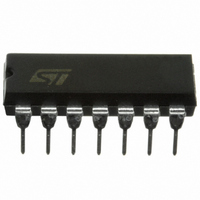
IC FLIP FLOP DUAL D-TYPE 14-DIP
Manufacturer
STMicroelectronics
Series
4000Br
Type
D-Typer
Specifications of HCF4013BEY
Function
Set(Preset) and Reset
Output Type
Differential
Number Of Elements
2
Number Of Bits Per Element
1
Frequency - Clock
24MHz
Delay Time - Propagation
45ns
Trigger Type
Positive Edge
Current - Output High, Low
6.8mA, 6.8mA
Voltage - Supply
3 V ~ 20 V
Operating Temperature
-55°C ~ 125°C
Mounting Type
Through Hole
Package / Case
14-DIP (0.300", 7.62mm)
Number Of Circuits
2
Logic Family
HCF40
Logic Type
D-Type Flip-Flop
Polarity
Inverting/Non-Inverting
Input Type
Single-Ended
Propagation Delay Time
300 ns
High Level Output Current
- 2.4 mA
Low Level Output Current
2.4 mA
Supply Voltage (max)
20 V
Maximum Operating Temperature
+ 125 C
Mounting Style
Through Hole
Minimum Operating Temperature
- 55 C
Supply Voltage (min)
3 V
Circuit Type
Monolithic Integrated
Current, Supply
600 μA
Function Type
D-Type
Logic Function
Flip-Flop
Package Type
DIP-14
Special Features
Medium Speed
Temperature, Operating, Range
-55 to +125 °C
Voltage, Supply
3 to 20 V
Lead Free Status / RoHS Status
Lead free / RoHS Compliant
Other names
497-1346-5
Available stocks
Company
Part Number
Manufacturer
Quantity
Price
Company:

Part Number:
HCF4013BEY
Manufacturer:
ST
Quantity:
12 000


HCF4013B
DYNAMIC ELECTRICAL CHARACTERISTICS (T
(*) Typical temperature coefficient for all V
(1) Input tr, tf = 5ns
(2) If more than unit is cascaded in a parallel clocked application, tr should be made less than or equal to the sum of the fixed propagation
delay time at 15pF and the transition time of the carry output driving stage for the estimated capacitive load.
4/9
t
t
Symbol
TLH
THL
t
f
r
t
CL
t
t
setup
, t
PLH
PHL
t
t
W
W
f
t
t
(1)
THL
TLH
(2)
Propagation Delay Time
(CLOCK to Q or Q outputs)
Propagation Delay Time
(SET to Q or RESET to Q)
Propagation Delay
Time(SET to Q or RESET
to Q)
Transition Time
Maximum Clock Input
Frequency
Clock Pulse Width
Clock Input Rise or Fall
Time
Set or Reset Pulse Width
Data Setup Time
Parameter
DD
value is 0.3 %/°C.
V
DD
10
15
10
15
10
15
10
15
10
15
10
15
10
15
10
15
10
15
5
5
5
5
5
5
5
5
5
(V)
Test Condition
amb
= 25°C, C
L
= 50pF, R
L
= 200K , t
Min.
140
180
3.5
12
60
40
80
50
40
20
15
8
Value (*)
Typ.
150
150
200
100
65
45
65
45
85
60
50
40
16
24
70
30
20
90
40
25
20
10
7
7
r
= t
Max.
300
130
300
130
400
170
120
200
100
90
90
80
15
f
4
1
= 20 ns)
MHz
Unit
ns
ns
ns
ns
ns
ns
ns
s
Related parts for HCF4013BEY
Image
Part Number
Description
Manufacturer
Datasheet
Request
R

Part Number:
Description:
NAND GATES
Manufacturer:
STMICROELECTRONICS [STMicroelectronics]
Datasheet:

Part Number:
Description:
STMicroelectronics [RIPPLE-CARRY BINARY COUNTER/DIVIDERS]
Manufacturer:
STMicroelectronics
Datasheet:
Part Number:
Description:
STMicroelectronics [LIQUID-CRYSTAL DISPLAY DRIVERS]
Manufacturer:
STMicroelectronics
Datasheet:

Part Number:
Description:
BOARD EVAL FOR MEMS SENSORS
Manufacturer:
STMicroelectronics
Datasheet:
Part Number:
Description:
NPN TRANSISTOR POWER MODULE
Manufacturer:
STMicroelectronics
Datasheet:
Part Number:
Description:
TURBOSWITCH ULTRA-FAST HIGH VOLTAGE DIODE
Manufacturer:
STMicroelectronics
Datasheet:
Part Number:
Description:
Manufacturer:
STMicroelectronics
Datasheet:
Part Number:
Description:
DIODE / SCR MODULE
Manufacturer:
STMicroelectronics
Datasheet:
Part Number:
Description:
DIODE / SCR MODULE
Manufacturer:
STMicroelectronics
Datasheet:
Part Number:
Description:
Search -----> STE16N100
Manufacturer:
STMicroelectronics
Datasheet:
Part Number:
Description:
Search ---> STE53NA50
Manufacturer:
STMicroelectronics
Datasheet:
Part Number:
Description:
NPN Transistor Power Module
Manufacturer:
STMicroelectronics
Datasheet: