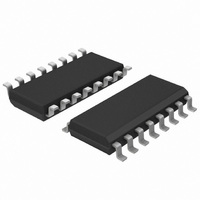
74HC174D,652 NXP Semiconductors, 74HC174D,652 Datasheet - Page 13

74HC174D,652
Manufacturer Part Number
74HC174D,652
Description
IC HEX D F-F POS-EDGE 16-SOIC
Manufacturer
NXP Semiconductors
Series
74HCr
Type
D-Type Busr
Datasheets
1.74HCT4046ADB112.pdf
(19 pages)
2.74HCT4046ADB112.pdf
(23 pages)
3.74HCT174N652.pdf
(13 pages)
Specifications of 74HC174D,652
Output Type
Inverted
Package / Case
16-SOIC (3.9mm Width)
Function
Master Reset
Number Of Elements
1
Number Of Bits Per Element
6
Frequency - Clock
107MHz
Delay Time - Propagation
16ns
Trigger Type
Positive Edge
Voltage - Supply
2 V ~ 6 V
Operating Temperature
-40°C ~ 125°C
Mounting Type
Surface Mount
Number Of Circuits
7
Logic Family
74HC
Logic Type
D-Type Flip-Flop
Polarity
Non-Inverting
Input Type
Single-Ended
Propagation Delay Time
17 ns
High Level Output Current
- 5.2 mA
Low Level Output Current
5.2 mA
Supply Voltage (max)
6 V
Maximum Operating Temperature
+ 125 C
Mounting Style
SMD/SMT
Minimum Operating Temperature
- 40 C
Supply Voltage (min)
2 V
Lead Free Status / RoHS Status
Lead free / RoHS Compliant
Current - Output High, Low
-
Lead Free Status / Rohs Status
Lead free / RoHS Compliant
Other names
568-2628-5
933714570652
933714570652
Philips Semiconductors
AC waveforms 74HCT
Test circuit for 74HCT
March 1988
handbook, full pagewidth
HCMOS family characteristics
C
R
(1) In Fig.9 the active transition of the clock is going from LOW-to-HIGH and the active level of the forcing signals
(2) For AC measurements: t
Fig.9
L
T
(SET, RESET and PRESET) is HIGH. The actual direction of the transition of the clock input and the actual
active levels of the forcing signals are specified in the individual device data sheet.
=
=
Set-up times, hold times, removal times, propagation delays and the maximum clock pulse frequency for
sequential logic ICs.
load capacitance including jig and probe capacitance (see AC
CHARACTERISTICS for values).
termination resistance should be equal to the output impedance Z
the pulse generator.
OUTPUT
PRESET
CLOCK
RESET,
r
INPUT
INPUT
INPUT
DATA
SET,
= t
f
= 6 ns; when measuring f
handbook, halfpage
GENERATOR
10%
1.3 V
PULSE
t su
t rem
1.3 V
t r
10%
1.3 V
t PLH
90%
t WH
max
Fig.10 Test circuit.
1.3 V
V I
90%
t h
, there is no constraint on t
1/f max
t TLH
t f
R T
13
t WL
o
D.U.T
V CC
t su
of
t PHL
V O
r
, t
f
with 50% duty factor.
C L
t h
FAMILY SPECIFICATIONS
t THL
MGK565
50 pF
MGK568
3 V
GND
3 V
GND
3 V
GND


