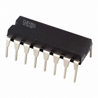
HEF4049BP,652 NXP Semiconductors, HEF4049BP,652 Datasheet - Page 5

HEF4049BP,652
Manufacturer Part Number
HEF4049BP,652
Description
IC INVERTER HEX 1INPUT 16DIP
Manufacturer
NXP Semiconductors
Series
4000Br
Datasheet
1.HEF4049BP652.pdf
(11 pages)
Specifications of HEF4049BP,652
Logic Type
Inverter
Package / Case
16-DIP (0.300", 7.62mm)
Number Of Inputs
1
Number Of Circuits
6
Current - Output High, Low
4.2mA, 4.2mA
Voltage - Supply
3 V ~ 15 V
Operating Temperature
-40°C ~ 125°C
Mounting Type
Through Hole
Logic Family
HE4000B
Number Of Channels Per Chip
6
Polarity
Inverting
Supply Voltage (max)
15 V
Supply Voltage (min)
3 V
Maximum Operating Temperature
85 C
Mounting Style
SMD/SMT
High Level Output Current
- 3.6 mA (Min)
Input Bias Current (max)
16 uA
Low Level Output Current
24 mA (Min)
Maximum Power Dissipation
750 mW
Minimum Operating Temperature
- 40 C
Number Of Lines (input / Output)
6 / 6
Propagation Delay Time
50 ns
Lead Free Status / RoHS Status
Lead free / RoHS Compliant
Lead Free Status / RoHS Status
Lead free / RoHS Compliant, Lead free / RoHS Compliant
Other names
568-1686-5
933277650652
HEF4049BPN
933277650652
HEF4049BPN
NXP Semiconductors
11. Dynamic characteristics
Table 7.
V
[1]
Table 8.
P
HEF4049B_8
Product data sheet
Symbol
t
t
t
t
Symbol
P
PHL
PLH
THL
TLH
SS
D
D
can be calculated from the formulas shown. V
= 0 V; C
The typical values of the propagation delay and transition times are calculated from the extrapolation formulas shown (C
Parameter
HIGH to LOW
propagation delay
LOW to HIGH
propagation delay
HIGH to LOW output
transition time
LOW to HIGH output
transition time
Dynamic characteristics
Dynamic power dissipation P
Parameter
dynamic power
dissipation
L
= 50 pF; t
r
= t
f
≤
20 ns; T
V
10 V
15 V
5 V
DD
Conditions
nA to nY;
see
nA to nY;
see
see
see
amb
Figure 5
Figure 5
Figure 5
Figure 5
= 25
Typical formula for P
P
P
P
D
D
D
D
= 2500 × f
= 11000 × f
= 35000 × f
°
C; unless otherwise specified.
SS
Rev. 08 — 2 December 2009
= 0 V; t
V
10 V
15 V
10 V
15 V
10 V
15 V
10 V
15 V
5 V
5 V
5 V
5 V
DD
i
+ Σ(f
i
i
+ Σ(f
+ Σ(f
r
[1]
[1]
[1]
[1]
= t
o
f
o
o
× C
≤
Extrapolation formula
26 ns + (0.18 ns/pF)C
11 ns + (0.08 ns/pF)C
23 ns + (0.55 ns/pF)C
14 ns + (0.23 ns/pF)C
12 ns + (0.16 ns/pF)C
10 ns + (1.00 ns/pF)C
× C
× C
D
9 ns + (0.05 ns/pF)C
3 ns + (0.35 ns/pF)C
3 ns + (0.14 ns/pF)C
2 ns + (0.09 ns/pF)C
9 ns + (0.42 ns/pF)C
6 ns + (0.28 ns/pF)C
20 ns; T
(μW)
L
) × V
L
L
) × V
) × V
DD
amb
DD
DD
2
2
2
= 25
°
C.
where:
f
f
C
V
Σ(f
i
o
L
L
L
L
L
L
L
L
L
L
L
L
DD
= input frequency in MHz;
L
= output frequency in MHz;
o
= output load capacitance in pF;
× C
= supply voltage in V;
L
Min
-
-
-
-
-
-
-
-
-
-
-
-
) = sum of the outputs.
Hex inverting buffers
HEF4049B
Typ
35
15
12
50
25
20
20
10
60
30
20
7
© NXP B.V. 2009. All rights reserved.
Max
100
120
70
30
25
50
40
40
20
14
60
40
L
in pF).
Unit
ns
ns
ns
ns
ns
ns
ns
ns
ns
ns
ns
ns
5 of 11


