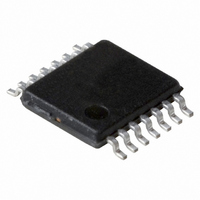
74HC164PW,118 NXP Semiconductors, 74HC164PW,118 Datasheet - Page 9

74HC164PW,118
Manufacturer Part Number
74HC164PW,118
Description
IC 8BIT SHIFT REGISTER 14TSSOP
Manufacturer
NXP Semiconductors
Series
74HCr
Type
Not Requiredr
Datasheet
1.74HC164D653.pdf
(20 pages)
Specifications of 74HC164PW,118
Package / Case
14-TSSOP
Logic Type
Shift Register
Function
Serial to Parallel
Output Type
Standard
Number Of Elements
1
Number Of Bits Per Element
8
Voltage - Supply
2 V ~ 6 V
Operating Temperature
-40°C ~ 125°C
Mounting Type
Surface Mount
Counting Sequence
Serial to Parallel
Number Of Circuits
1
Logic Family
HC
Propagation Delay Time
12 ns
Supply Voltage (max)
6 V
Maximum Operating Temperature
+ 125 C
Minimum Operating Temperature
- 40 C
Mounting Style
SMD/SMT
Supply Voltage (min)
2 V
Technology
CMOS
Number Of Elements
1
Number Of Bits
8
Logical Function
Shift Register
Operating Supply Voltage (typ)
5V
Package Type
TSSOP
Operating Temp Range
-40C to 125C
Operating Supply Voltage (min)
2V
Operating Supply Voltage (max)
6V
Operating Temperature Classification
Automotive
Mounting
Surface Mount
Pin Count
14
Lead Free Status / RoHS Status
Lead free / RoHS Compliant
Lead Free Status / RoHS Status
Lead free / RoHS Compliant, Lead free / RoHS Compliant
Other names
74HC164PW-T
74HC164PW-T
935187370118
74HC164PW-T
935187370118
Available stocks
Company
Part Number
Manufacturer
Quantity
Price
Company:
Part Number:
74HC164PW,118
Manufacturer:
NXP Semiconductors
Quantity:
2 000
NXP Semiconductors
Table 7.
GND = 0 V; t
[1]
[2]
[3]
Table 8.
74HC_HCT164
Product data sheet
Symbol Parameter
C
Type
74HC164
74HCT164
Fig 7.
PD
t
t
C
P
f
f
C
V
N = number of inputs switching;
(C
pd
t
i
o
D
CC
PD
L
is the same as t
(1) Measurement points are given in
= input frequency in MHz;
= output frequency in MHz;
is the same as t
= output load capacitance in pF;
= C
is used to determine the dynamic power dissipation (P
= supply voltage in V;
L
V
V
Waveforms showing the clock (CP) to output (Qn) propagation delays, the clock pulse width, the output
transition times and the maximum clock frequency
power
dissipation
capacitance
PD
OL
Dynamic characteristics
Measurement points
r
CC
V
= t
and V
2
CC
f
f
= 6 ns; C
2
o
) = sum of outputs.
OH
f
THL
PHL
i
are typical voltage output levels that occur with the output load.
N + (C
and t
and t
Input
V
0.5V
1.3 V
L
M
Conditions
per package;
V
TLH
= 50 pF; test circuit see
I
PLH
= GND to V
CC
.
.
Qn output
L
CP input
V
CC
…continued
2
Table
f
CC
GND
V
V
All information provided in this document is subject to legal disclaimers.
o
OH
OL
) where:
V
1.5 V
I
8.
Rev. 5 — 25 November 2010
Output
V
0.5V
1.3 V
t
THL
M
Figure
V
t
V
PHL
M
Y
CC
[3]
t
D
W
in W):
V
Min Typ Max
10; unless otherwise specified
M
V
1/f
-
X
max
25 C
40
t
TLH
-
t
PLH
V
0.1V
0.1V
74HC164; 74HCT164
X
40 C to +85 C
8-bit serial-in, parallel-out shift register
Min
CC
CC
-
001aal392
Max
-
40 C to +125 C Unit
Min
V
0.9V
0.9V
-
Y
© NXP B.V. 2010. All rights reserved.
CC
CC
Max
-
pF
9 of 20


