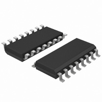
74LV165D,118 NXP Semiconductors, 74LV165D,118 Datasheet - Page 2

74LV165D,118
Manufacturer Part Number
74LV165D,118
Description
IC 8BIT SHIFT REGISTER 16SOIC
Manufacturer
NXP Semiconductors
Series
74LVr
Datasheet
1.74LV165N112.pdf
(14 pages)
Specifications of 74LV165D,118
Package / Case
16-SOIC (3.9mm Width)
Logic Type
Shift Register
Function
Parallel or Serial to Serial
Output Type
Differential
Number Of Elements
1
Number Of Bits Per Element
8
Voltage - Supply
1 V ~ 5.5 V
Operating Temperature
-40°C ~ 125°C
Mounting Type
Surface Mount
Counting Sequence
Serial/Parallel to Serial
Number Of Circuits
1
Logic Family
LV
Propagation Delay Time
18 ns
Supply Voltage (max)
5.5 V
Maximum Operating Temperature
+ 125 C
Minimum Operating Temperature
- 40 C
Mounting Style
SMD/SMT
Supply Voltage (min)
1 V
Lead Free Status / RoHS Status
Lead free / RoHS Compliant
Lead Free Status / RoHS Status
Lead free / RoHS Compliant, Lead free / RoHS Compliant
Other names
74LV165D-T
74LV165D-T
935156060118
74LV165D-T
935156060118
1. C
Philips Semiconductors
FEATURES
QUICK REFERENCE DATA
GND = 0 V; T
NOTES:
ORDERING INFORMATION
PIN CONFIGURATION
t
f
C
C
16-Pin Plastic DIL
16-Pin Plastic SO
16-Pin Plastic SSOP Type II
16-Pin Plastic TSSOP Type I
1998 May 07
PHL
max
SYMBOL
Wide operating voltage: 1.0 to 5.5 V
Optimized for low voltage applications: 1.0 to 3.6 V
Accepts TTL input levels between V
Typical V
T
Typical V
T
Asynchronous 8-bit parallel load
Synchronous serial input
Output capability: standard
I
8-bit parallel-in/serial-out shift register
I
PD
CC
P
f
f
amb
amb
i
o
PD
D
= input frequency in MHz; C
/t
= output frequency in MHz; V
(C
category: MSI
PLH
= C
= 25 C
= 25 C
L
is used to determine the dynamic power dissipation (P
PD
OLP
OHV
V
PACKAGES
CC
amb
Propagation delay
CE, CP to Q
PL to Q
D
Maximum clock frequency
Input capacitance
Power dissipation capacitance per gate
V
(output ground bounce) < 0.8 V at V
2
(output V
7
CC
= 25 C; t
to Q
GND
f
CP
2
PL
D
D
D
D
Q
o
) = sum of the outputs.
4
5
6
7
7
7
7
, Q
f
, Q
i
2
3
4
5
6
7
8
1
) (C
OH
7
7
r
7
= t
, Q
undershoot) > 2 V at V
PARAMETER
f
7
L
2.5 ns
L
= output load capacitance in pF;
CC
V
CC
CC
= supply voltage in V;
2
TEMPERATURE RANGE
SV00585
= 2.7 V and V
16
15
14
12
11
10
13
9
f
o
–40 C to +125 C
–40 C to +125 C
–40 C to +125 C
–40 C to +125 C
) where:
V
CE
D
D
D
D
D
Q
CC
3
2
1
0
S
7
CC
CC
= 3.3 V,
= 3.3 V,
CC
= 3.6 V
C
V
V
V
D
L
CC
CC
I
= GND to V
= 15 pF;
in W)
= 3.3 V
= 3.3 V
OUTSIDE NORTH AMERICA
2
CONDITIONS
DESCRIPTION
The 74LV165 is a low-voltage Si-gate CMOS device and is pin and
function compatible with 74HC/HCT165.
The 74LV165 is an 8-bit parallel-load or serial-in shift register with
complementary serial outputs (Q
stage. When the parallel load (PL) input is LOW, parallel data from the
D
is HIGH, data enters the register serially at the D
place to the right (Q
transition. This feature allows parallel-to-serial converter expansion by
tying the Q
The clock input is a gated-OR structure which allows one input to be
used as an active LOW clock enable (CE) input. The pin assignment
for the CP and CE inputs is arbitrary and can be reversed for layout
convenience. The LOW-to-HIGH transition of input CE should only
take place while CP HIGH for predictable operation. Either the CP or
the CE should be HIGH before the LOW-to-HIGH transition of PL to
prevent shifting the data when PL is activated.
CC
PIN DESCRIPTION
1
2
7
8
9
10
11, 12, 13, 14, 3, 4, 5, 6
15
16
0
74LV165 DB
74LV165 PW
1
74LV165 N
74LV165 D
to D
PIN NUMBER
7
inputs are loaded into the register asynchronously. When PL
7
output to the D
0
Q
1
NORTH AMERICA
PL
CP
Q
GND
Q
D
D
CE
V
SYMBOL
S
Q
74LV165PW DH
CC
S
0
7
7
input of the succeeding stage.
2
74LV165 DB
to D
, etc.) with each positive-going clock
74LV165 N
74LV165 D
7
TYPICAL
and Q
7
3.5
18
18
14
78
35
Asynchronous parallel load
input (active LOW)
Clock input (LOW to
HIGH, edge-triggered)
Complementary output from
the last stage
Ground (0 V)
Serial output from last stage
Serial data input
Parallel data inputs
Clock enable input
(active LOW)
Positive supply voltage
7
) available from the last
Product specification
FUNCTION
S
input and shifts one
74LV165
853–1915 19349
PKG. DWG. #
SOT109-1
SOT338-1
SOT403-1
SOT38-4
UNIT
MHz
pF
pF
ns


